LTC1553CSW Просмотр технического описания (PDF) - Linear Technology
Номер в каталоге
Компоненты Описание
Список матч
LTC1553CSW
Linear Technology

LTC1553CSW Datasheet PDF : 24 Pages
| |||
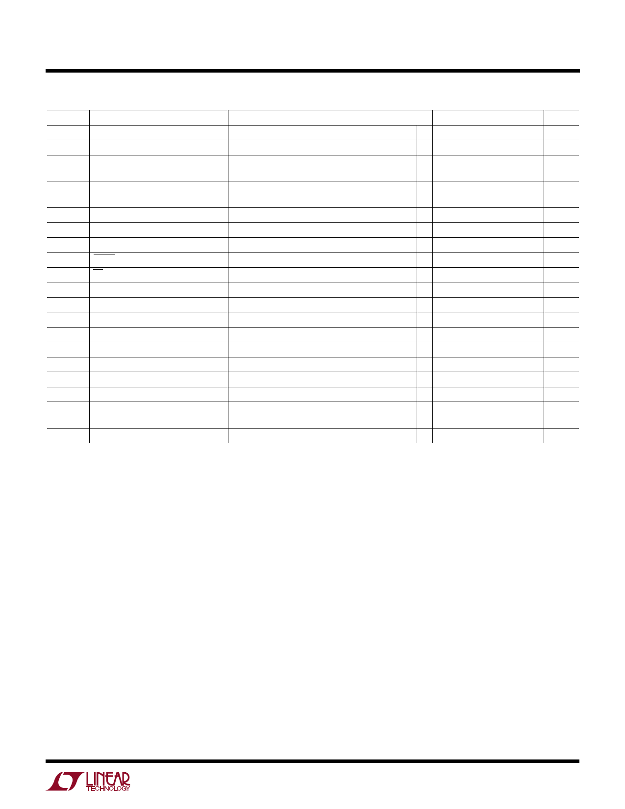
LTC1553
ELECTRICAL CHARACTERISTICS VCC = 5V, PVCC = 12V, TA = 25°C, unless otherwise noted. (Note 3)
SYMBOL PARAMETER
CONDITIONS
MIN TYP MAX
IIMAX
ISS
ISSIL
ISSHIL
IMAX Sink Current
Soft Start Source Current
Maximum Soft Start Sink Current
Under Current Limit
Soft Start Sink Current Under Hard
Current Limit
VIMAX = VCC
VSS = 0V, VIMAX = 0V, VIFB = VCC
VSENSE = VOUT, VIMAX = VCC, VIFB = 0V
(Notes 8, 9), VSS = VCC
VSENSE = 0V, VIMAX = VCC, VIFB = 0V
q 150
180
220
q – 13 – 10
–7
q 30
60
150
q 20
45
tSSHIL
tPWRGD
tPWRBAD
tFAULT
tOT
VOT
VOTDD
VSHDN
tr, tf
t NOL
DCMAX
VIH
VIL
RIN
Hard Current Limit Hold Time
Power Good Response Time↑
Power Good Response Time↓
FAULT Response Time
OT Response Time
Over-Temperature Trip Point
Over-Temperature Driver Disable
Shutdown
Driver Rise and Fall Time
Driver Nonoverlap Time
Maximum G1 Duty Cycle
VID0 to VID4 Input High Voltage
VID0 to VID4 Input Low Voltage
VID0 to VID4 Internal Pull-Up
Resistance
VSENSE = 0V, VIMAX = 4V, VIFB↓ from 5V (Note 4)
VSENSE↑ from 0V to Rated VOUT
VSENSE↓ from Rated VOUT to 0V
VSENSE↑ from Rated VOUT to VCC
OUTEN↓, VID0 to VID4 = 0 (Note 10) (Figure 3)
OUTEN↓, VID0 to VID4 = 0 (Note 10) (Figure 3)
OUTEN↓, VID0 to VID4 = 0 (Note 10) (Figure 3)
OUTEN↓, VID0 to VID4 = 0 (Note 10) (Figure 3)
(Figure 4)
(Figure 4)
(Figure 4)
q 0.5
q 200
q 200
q 15
q 1.9
q 1.6
q
q
q 30
q 77
q2
q
q 10
500
1
2
500 1000
500 1000
40
60
2
2.12
1.7
1.8
0.8
90
150
100
84
88
0.8
20
ISINK
Digital Output Sink Current
q 10
UNITS
µA
µA
µA
mA
µs
ms
µs
µs
µs
V
V
V
ns
ns
%
V
V
kΩ
mA
The q denotes specifications which apply over the full operating
temperature range.
Note 1: Absolute Maximum Ratings are those values beyond which the life
of a device may be impaired.
Note 2: When IFB is taken below GND, it will be clamped by an internal
diode. This pin can handle input currents greater than 100mA below GND
without latchup. In the positive direction, it is not clamped to VCC or PVCC.
Note 3: All currents into device pins are positive; all currents out of the
device pins are negative. All voltages are referenced to ground unless
otherwise specified.
Note 4: This parameter is guaranteed by correlation and is not tested
directly.
Note 5: The LTC1553 goes into the shutdown mode if VID0 to VID4 are
floating. Due to the internal pull-up resistors, there will be an additional
0.25mA/pin if any of the VID0 to VID4 pins are pulled low.
Note 6: Supply current in normal operation is dominated by the current
needed to charge and discharge the external FET gates. This will vary with
the LTC1553 operating frequency, supply voltage and the external FETs
used.
Note 7: The open-loop DC gain and transconductance from the SENSE pin to
COMP pin will be (GERR)(1.265/3.3) and (gmERR)(1.265/3.3) respectively.
Note 8: The current limiting amplifier can sink but cannot source current.
Under normal (not current limited) operation, the output current will be zero.
Note 9: Under typical soft current limit, the net soft start discharge current
will be 60µA (ISSIL) + [– 10µA(ISS)] = 50µA. The soft start sink-to-source
current ratio is designed to be 6:1.
Note 10: When VID0 to VID4 are all HIGH, the LTC1553 will be forced to
shut down internally. The OUTEN trip voltages are guaranteed by design for
all other input codes.
3
Share Link: