ISL976787IBZ-T Просмотр технического описания (PDF) - Intersil
Номер в каталоге
Компоненты Описание
Список матч
ISL976787IBZ-T Datasheet PDF : 24 Pages
| |||
ISL97687
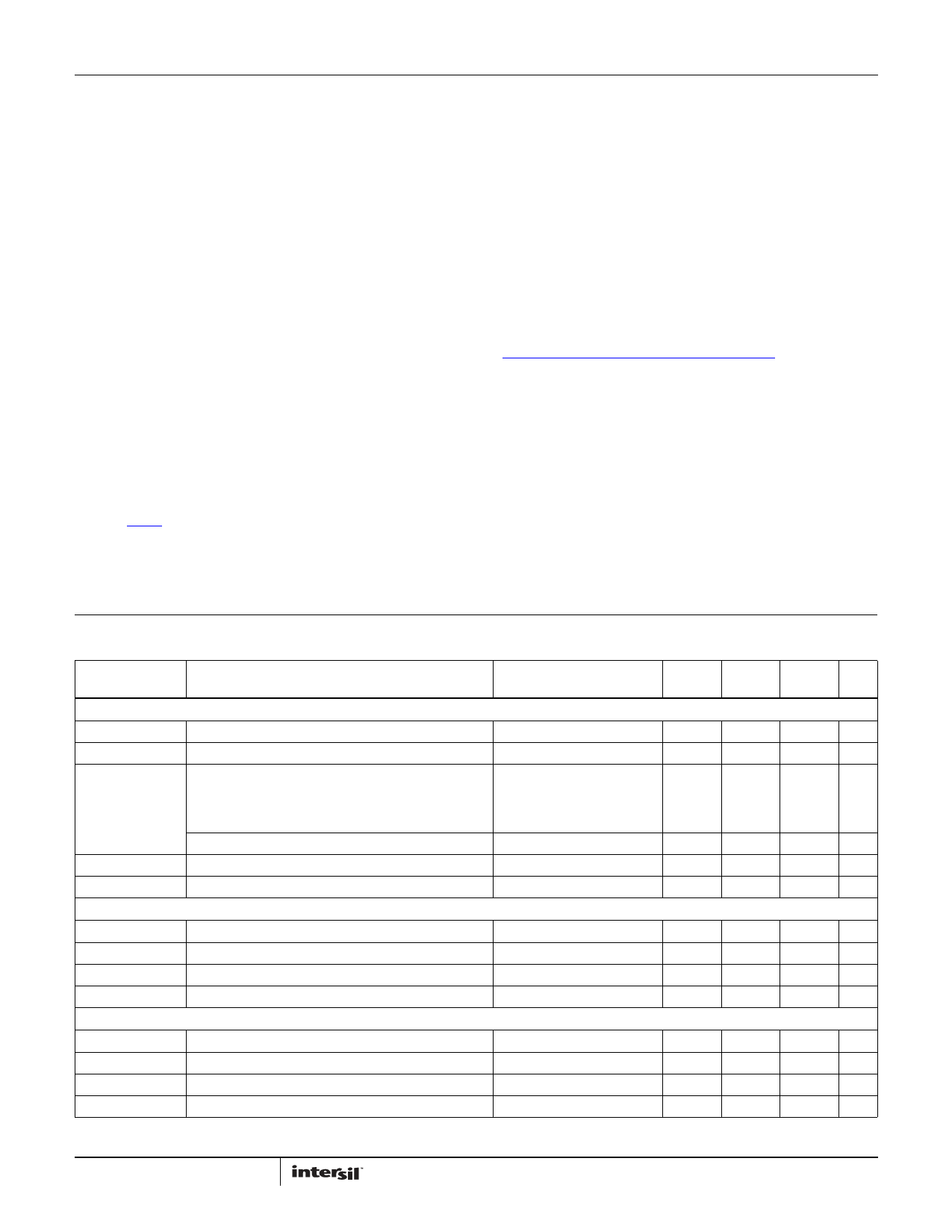
Absolute Maximum Ratings (TA = +25°C)
VIN, EN, PWMI, ACTL . . . . . . . . . . . . . . . . . . . . . . . . . . . . . . . . . . -0.3V to 45V
VDC. . . . . . . . . . . . . . . . . . . . . . . . . . . . . . . . . . . . . . . . . . . . . . . -0.3V to 5.75V
VLOGIC . . . . . . . . . . . . . . . . . . . . . . . . . . . . . . . . . . . . . . . . . . . . -0.3V to 2.75V
COMP, ISET1, ISET2, PWM_SET,
OSC, CS, OVP. . . . . . . . . . . . . . . . . . . . . . .-0.3V to min (VDC+0.3V, 5.75V)
EN_VSYNC, CSEL. . . . . . . . . . . . . . . . . . . . . . . . . . . . . . . . . . . . -0.3V to 5.75V
STV, EN_ADIM, EN_PS . . . . . . . . . . . . . . . . . . . . . . . . . . . . . . . -0.3V to 5.75V
CH1 - CH4 . . . . . . . . . . . . . . . . . . . . . . . . . . . . . . . . . . . . . . . . . . . -0.3V to 75V
GD, SLEW. . . . . . . . . . . . . . . . . . . . . . . . . . . . . . . . . . . . . . . . . . . . -0.3V to 18V
PGND . . . . . . . . . . . . . . . . . . . . . . . . . . . . . . . . . . . . . . . . . . . . . -0.3V to +0.3V
Above voltage ratings are all with respect to AGND pin
ESD Rating
Human Body Model (Tested per JESD22-A114F) . . . . . . . . . . . . . . . . 2kV
Machine Model (Tested per JESD22-A115C) . . . . . . . . . . . . . . . . . . 200V
Charged Device Model (JESD22-C101E) . . . . . . . . . . . . . . . . . . . . . . . 1kV
Latch Up (Tested per JESD-78B; Class 2, Level A) . . . . . . . . . . . . . . 100mA
Thermal Information
Thermal Resistance
θJA (°C/W) θJC (°C/W)
28 Ld TQFN (4 layer + vias, Notes 4, 5) . . .
32
4
28 Ld SOIC (4 layer, Notes 4, 6) . . . . . . . . .
54
25
Thermal Characterization (Typical, Note 7)
PSIJT (°C/W)
28 Ld TQFN . . . . . . . . . . . . . . . . . . . . . . . . . . . . . . . . . . . .
1
28 Ld SOIC. . . . . . . . . . . . . . . . . . . . . . . . . . . . . . . . . . . . .
4
Maximum Continuous Junction Temperature . . . . . . . . . . . . . . . . .+125°C
Storage Temperature . . . . . . . . . . . . . . . . . . . . . . . . . . . . .-65°C to +150°C
Power Dissipation
TQFN (W) SOIC (W)
TA < +25°C . . . . . . . . . . . . . . . . . . . . . . . . . . . . 3.13
1.85
TA < +70°C . . . . . . . . . . . . . . . . . . . . . . . . . . . . 1.72
1.02
TA < +85°C . . . . . . . . . . . . . . . . . . . . . . . . . . . . 1.25
0.74
TA < +105°C . . . . . . . . . . . . . . . . . . . . . . . . . . . 0.63
0.37
Pb-Free Reflow Profile . . . . . . . . . . . . . . . . . . . . . . . . . . . . . . . see link below
http://www.intersil.com/pbfree/Pb-FreeReflow.asp
Operating Conditions
Temperature Range . . . . . . . . . . . . . . . . . . . . . . . . . . . . . . .-40°C to +105°C
CAUTION: Do not operate at or near the maximum ratings listed for extended periods of time. Exposure to such conditions may adversely impact product
reliability and result in failures not covered by warranty.
NOTES:
4. θJA is measured in free air with the component mounted on a high effective thermal conductivity test board with “direct attach” features. See Tech
Brief TB379.
5. For θJC, the “case temp” location is the center of the exposed metal pad on the package underside.
6. For θJC, the “case temp” location is taken at the package top center.
7. PSIJT is the PSI junction-to-top thermal characterization parameter. If the package top temperature can be measured with this rating then the die
junction temperature can be estimated more accurately than the θJC and θJC thermal resistance ratings.
Electrical Specifications All specifications below are characterized at TA = -40°C to +105°C; VIN = 12V, EN = 5V. Boldface limits apply
over the operating temperature range, -40°C to +105°C.
PARAMETER
DESCRIPTION
CONDITION
MIN
MAX
(Note 8) TYP (Note 8) UNIT
GENERAL
VIN
IVIN_STBY
IVIN_ACTIVE
Backlight Supply Voltage
VIN Shutdown Current
Switching
Non-switching
(Note 9)
EN = 0
RFPWM = 3.3kΩ,
ILED = 100mA,
fSW = 600kHz,
COUT_SW = 1nF
9
32
V
5
µA
10
13 mA
4
5.5 mA
VUVLO
Undervoltage Lock-out Threshold
VUVLO_HYS
Undervoltage Lock-out Hysteresis
LINEAR REGULATOR
2.9
3.3
V
300
mV
VDC
5V Analog Bias Regulator
VDC_DROP
VDC LDO Load Regulation Tolerance
VLOGIC
2.5V Logic Bias Regulator
VLOGIC_DROP
VLOGIC LDO Load Regulation Tolerance
BOOST SWITCH CONTROLLER
VIN > 6V
IVDC = 30mA
VIN > 6V
IVLOGIC = 30mA
4.8
5
5.1
V
71
100 mV
2.3
2.4
2.5
V
31
100 mV
tSS
ISW_LIMIT
tR
tF
Soft-Start
Boost FET Current Limit
Gate Rise Time
Gate Falling Time
RSENSE = 50mΩ
COUT_SW = 1000pF
COUT_SW = 1000pF
16
ms
3.1
3.4
3.8
A
20
ns
17.6
ns
6
FN7714.0
September 15, 2011
Share Link: 