ISL97646 Просмотр технического описания (PDF) - Intersil
Номер в каталоге
Компоненты Описание
Список матч
ISL97646 Datasheet PDF : 15 Pages
| |||

ISL97646
The efficiency of LDO is depended on the difference
between input voltage and output voltage, as well as the
output current:
η(%) = (VIN1 – VLDO_OUT) × ILDO_OUT × 100%
(EQ. 7)
The less difference between input and output voltage, the
higher efficiency it is. The minimum dropout voltage of LDO
of ISL97646 is 300mV.
The ceramic capacitors are recommended for the LDO input
and output capacitor. Larger capacitors help reduce noise
and deviation during transient load change.
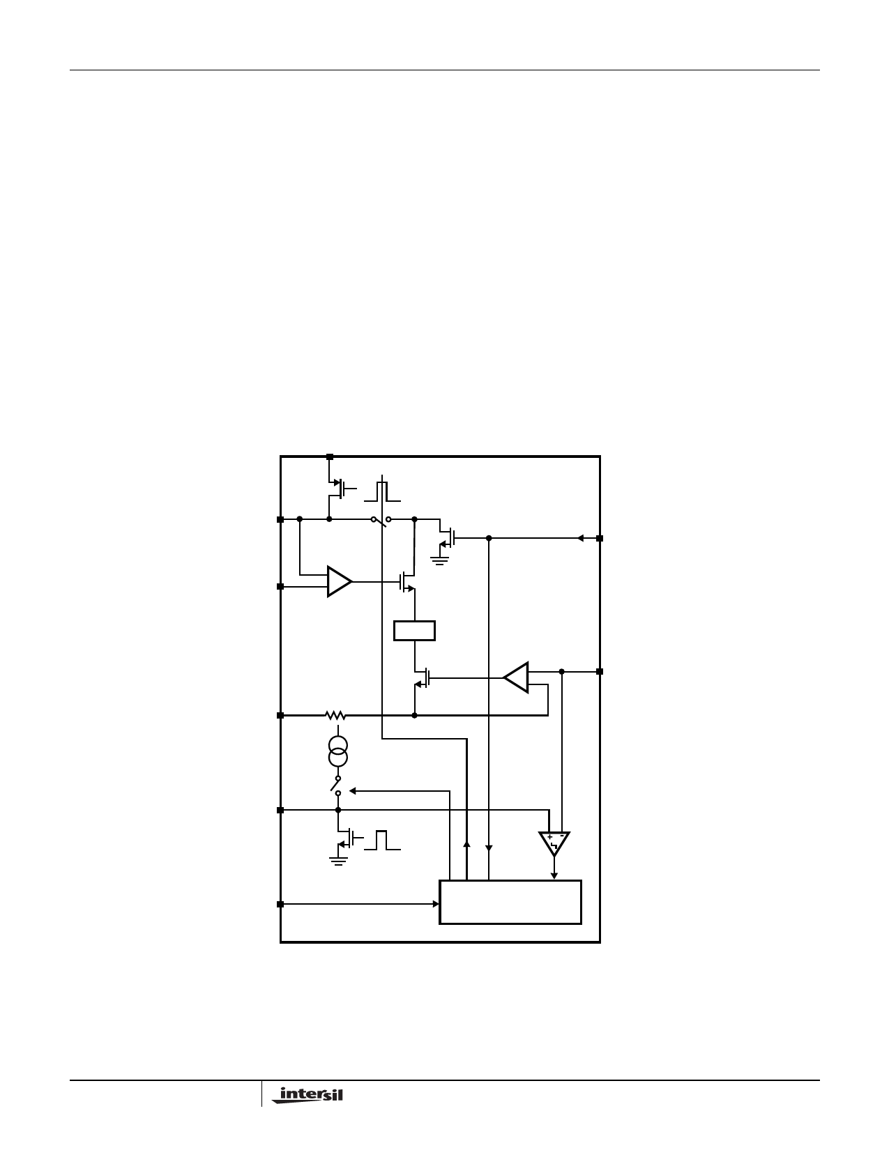
Gate Pulse Modulator Circuit
The gate pulse modulator circuit functions as a three way
multiplexer, switching VGHM between ground, VDD1 and
VGH. Voltage selection is provided by digital inputs VDPM
(enable) and VFLK (control). High to low delay and slew
control is provided by external components on pins CE and
RE, respectively. A block diagram of the gate pulse
modulator circuit is shown in Figure 16.
When VDPM is LOW, the block is disabled and VGHM is
grounded. When VDPM is HIGH, the output is determined
by VFLK. When VFLK goes high, VGHM is pulled to VGH by
a 70Ω switch. When VFLK goes low, there is a delay
controlled by capacitor CE, following which VGHM is driven
to VDD1, with a slew rate controlled by resistor RE. Note
that VDD1 is used only as a reference voltage for an
amplifier, thus does not have to source or sink a significant
DC current.
VGH
VGH_M
+
VDD1
-
x240
RE
200µA
CE
EnGPM1
+
VREF
-
VFLK
CONTROL AND
TIMING
FIGURE 16. GATE PULSE MODULATOR CIRCUIT BLOCK DIAGRAM
12
FN6265.1
December 14, 2007