IRU1261 Просмотр технического описания (PDF) - International Rectifier
Номер в каталоге
Компоненты Описание
Список матч
IRU1261 Datasheet PDF : 8 Pages
| |||
IRU1261
PIN DESCRIPTIONS
PIN # PIN SYMBOL
1
VCTRL
PIN DESCRIPTION
The control input pin of the regulator. This pin is connected, via a 10V resistor, to the 5V
supply to provide the base current for the pass transistor of both regulators. This allows
the regulator to have very low dropout voltage which allows one to generate a well regu-
lated 2.5V supply from the 3.3V input. A high frequency, 1mF capacitor is connected
between this pin and VIN pin to insure stability.
2
VOUT2
The output #2 (high current) of the regulator. A minimum of 100mF capacitor must be
connected from this pin to ground to insure stability.
3
Gnd
This pin is connected to ground. It is also the Tab of the package.
4
VIN
The power input pin of the regulator. Typically a large storage capacitor is connected from
this pin to ground to insure that the input voltage does not sag below the minimum drop
out voltage during the load transient response. This pin must always be higher than both
VOUT pins by the amount of the dropout voltage (see data sheet) in order for the device to
regulate properly.
5
VOUT1
The output #1 (low current) of the regulator. A minimum of 100mF capacitor must be
connected from this pin to ground to insure stability.
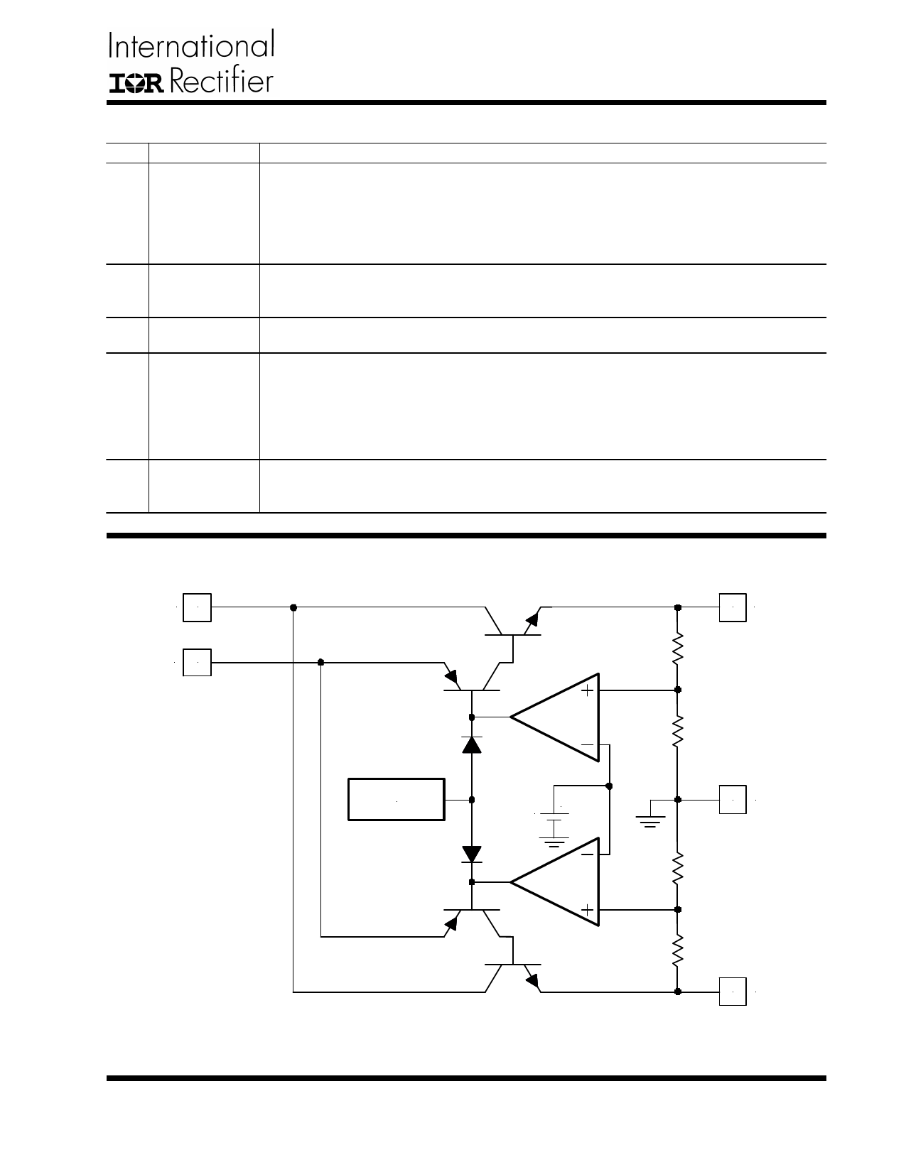
BLOCK DIAGRAM
VIN 4
VCTRL 1
5 VOUT1
THERMAL
SHUTDOWN
1.20V +
3 Gnd
Rev. 2.0
09/19/02
Figure 2 - Simplified block diagram of the IRU1261.
www.irf.com
2 VOUT2
3
Share Link: 