FM25C041 Просмотр технического описания (PDF) - Fairchild Semiconductor
Номер в каталоге
Компоненты Описание
Список матч
FM25C041 Datasheet PDF : 11 Pages
| |||
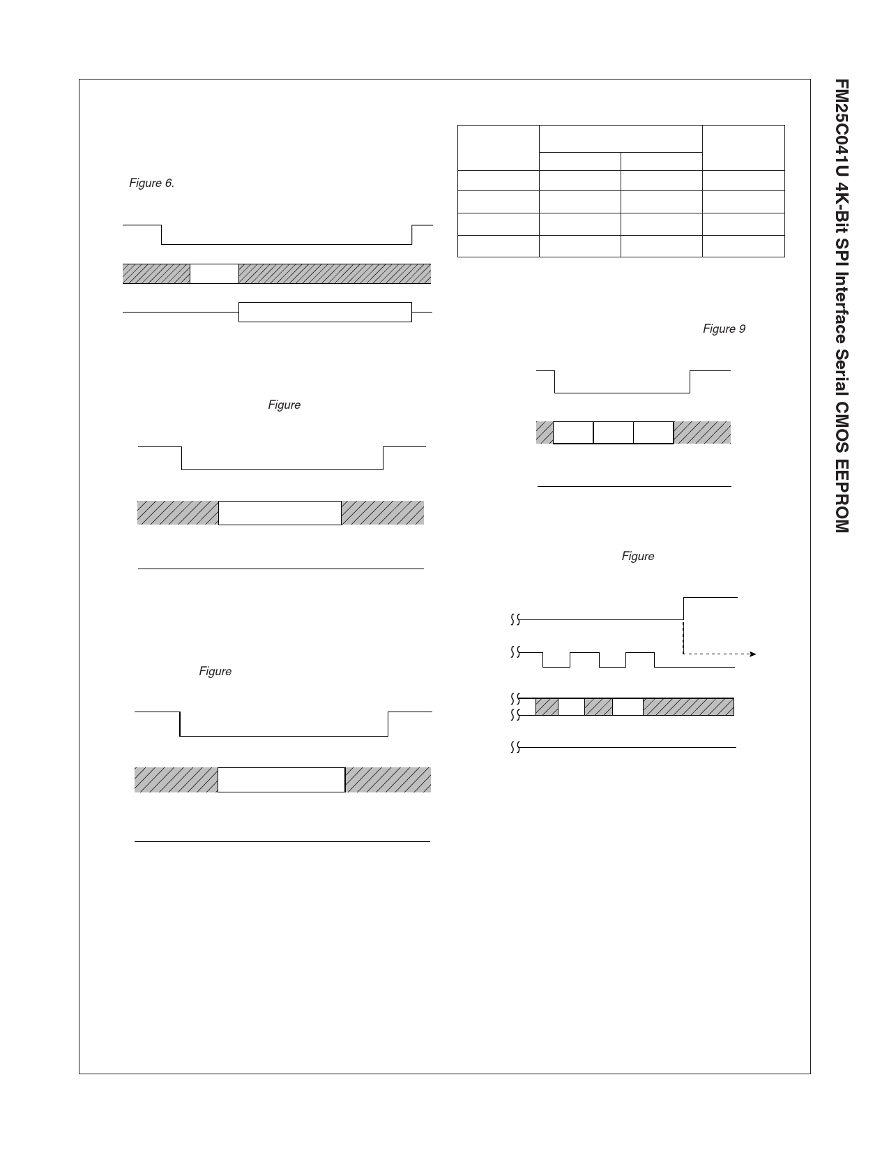
The RDSR command requires the following sequence. The /CS
pin is pulled low to select the EEPROM and then the RDSR
opcode is transmitted on the SI pin. After this is done, data on the
SI pin becomes don’t care. The data from the Status Register is
then shifted out on the SO pin starting with D7 bit first and D0 last.
See Figure 6.
FIGURE 6. Read Status Register
/CS
SI
RDSR
OP-CODE
SO
RDSR DATA
WRITE ENABLE (WREN):
When VCC is applied to the EEPROM, it “powers up” in a write-
disabled state. Therefore, all programming modes (Write to memory
array and Status register), must be preceded by a WRITE EN-
ABLE (WREN) instruction. See Figure 7.
FIGURE 7. Write Enable
/CS
SI
WREN Op-Code
SO
WRITE DISABLE (WRDI):
Executing this instruction disables all programming modes (Write
to memory array and Status register), preventing the EEPROM
from accidental writes. Once WRDI instruction is executed,
WREN instruction should be executed to re-enable all program-
ming modes. See Figure 8.
FIGURE 8. Write Disable
/CS
SI
WRDI Op-Code
SO
WRITE SEQUENCE (WRITE):
Write to the array is enabled only when /WP pin is held high and
the EEPROM is write enabled previously (via WREN instruction).
Also, the address of the memory location(s) to be programmed
must be outside the protected address field selected by the Block
Write Protection Level. See Table 4.
TABLE 4. Block Write Protection Levels
Level
0
Status Register Bits
BP1
0
BP0
0
Array
Address
Protected
None
1
0
1
180-1FF
2
1
0
100-1FF
3
1
1
000-1FF
A WRITE command requires the following sequence. The /CS pin
is pulled low to select the EEPROM, then the WRITE opcode is
transmitted on the SI pin followed by the byte address (A7-A0) and
followed by the data (D7-D0) to be written. See Figure 9.
FIGURE 9. Byte Write
/CS
SI
Write
Byte
Data
Op-Code Addr
High Z
SO
Internally, the programming will start after the /CS pin is brought
back to a high level. Note that the LOW to HIGH transition of the
/CS pin must occur during the SCK low time immediately after
clocking in the D0 data bit. See Figure 10.
FIGURE 10. Start of Programming
/CS
SCK
Start of internal
programming
SI D2
D1
D0
SO
High Z
Programming status (Busy/Ready) of the EEPROM can be deter-
mined by executing a READ STATUS REGISTER (RDSR) in-
struction after a write command. Upon executing the RDSR
instruction, if Bit 0 of the RDSR data is “1”, it indicates the WRITE
cycle is still in progress. If it is “0” then the WRITE cycle has ended.
Note that while the internal programming is still in progress (Bit 0
= 1), only the RDSR instruction is enabled. It is recommended that
no other instruction be issued till the internal programming is
complete.
FM25C041U Rev. B
8
www.fairchildsemi.com
Share Link: 