IDT7M1014S30GB Просмотр технического описания (PDF) - Integrated Device Technology
Номер в каталоге
Компоненты Описание
Список матч
IDT7M1014S30GB Datasheet PDF : 8 Pages
| |||
IDT7M1014 4K x 36 BiCMOS
DUAL-PORT STATIC RAM MODULE
MILITARY AND COMMERCIAL TEMPERATURE RANGES
AC ELECTRICAL CHARACTERISTICS
(VCC = 5V ± 10%, TA = –55°C to +125°C or 0°C to +70°C)
7M1014SxxG
-15
-20
Symbol Parameter
Read Cycle
Min. Max. Min. Max.
7M1014SxxGB
-25
-30
Min. Max. Min. Max. Unit
tRC
Read Cycle Time
15
—
20
—
25
—
tAA
Address Access Time
—
15
—
20
—
25
tOE
Output Enable Access Time
—
8
—
10
—
12
tOH
Output Hold from Address Change
3
—
3
—
3
—
tOLZ(1) Output Enable to Output in Low-Z
0
—
0
—
0
—
tOHZ(1) Output Disable to Output in Hi-Z
—
7
—
9
—
11
Write Cycle
tWC
Write Cycle Time
15
—
20
—
25
—
tAW
Address Valid to End of Write
14
—
15
—
20
—
tAS
Address Set-Up Time
0
—
0
—
0
—
tWP
Write Pulse Width
12
—
15
—
20
—
tWR
Write Recovery Time
1
—
2
—
2
—
tDW
Data Valid to End of Write
10
—
12
—
15
—
tDH
Data Hold Time
0
—
0
—
0
—
tWHZ(1) Write Enable to Output in Hi-Z
—
7
—
9
—
11
tOW(1)
Output Active from End of Write
0
—
0
—
0
—
tWDD
Write Pulse to Data Delay
—
30
—
40
—
45
tDDD(1) Write Data Valid to Read Data Delay
—
25
—
30
—
35
NOTES:
1. This parameter is guaranteed by design but not tested.
2. Port-to-Port delay through the RAM cells from the writing port to the reading port.
30
—
ns
—
30
ns
—
15
ns
3
—
ns
0
—
ns
—
13
ns
30
—
ns
25
—
ns
0
—
ns
25
—
ns
2
—
ns
20
—
ns
0
—
ns
—
13
ns
0
—
ns
—
50
ns
—
40
ns
2819 tbl 09
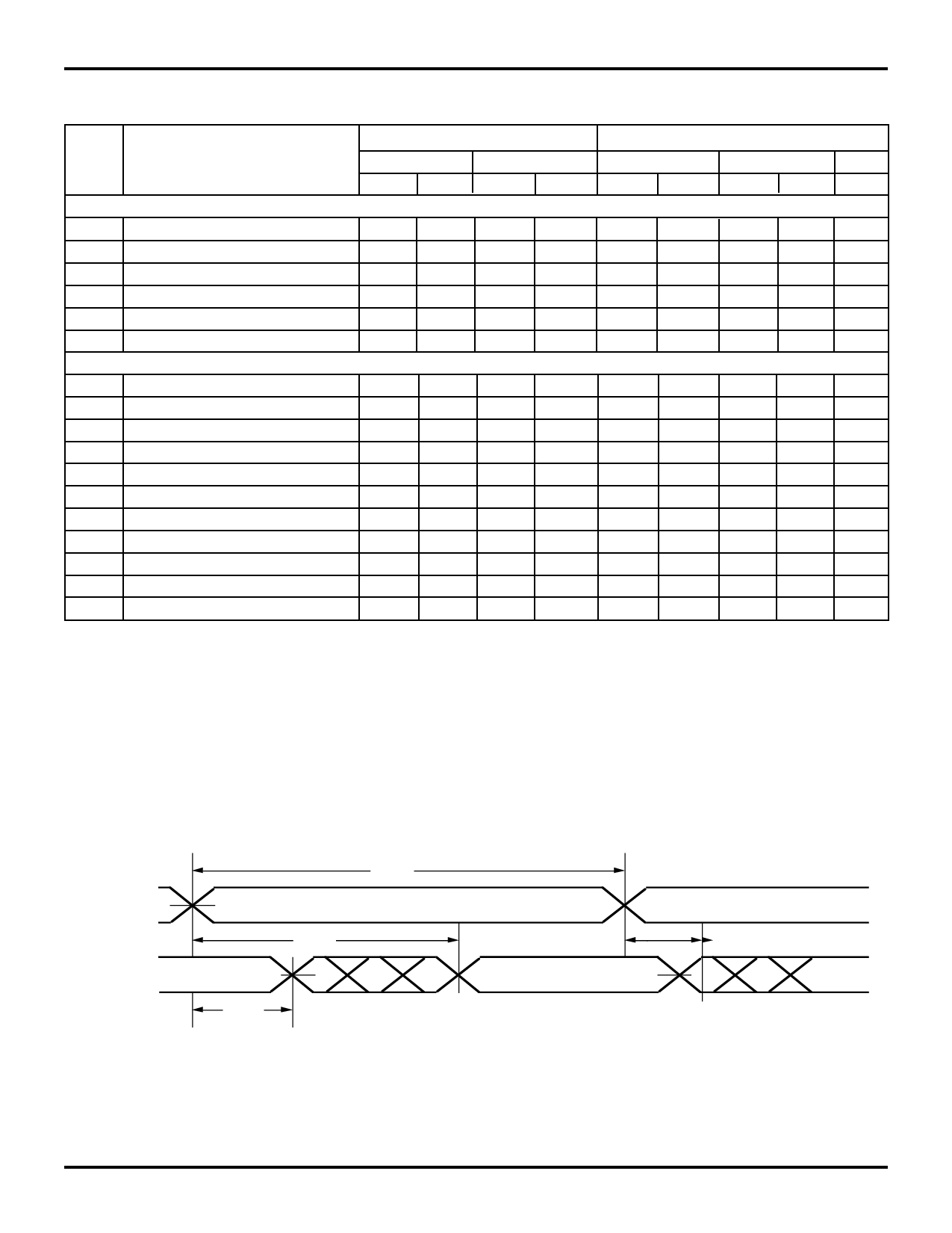
TIMING WAVEFORM OF READ CYCLE NO. 1 (EITHER SIDE) (1,2)
ADDRESS
DATAOUT
tRC
tAA
tOH
NOTES:
1. R/W is HIGH for Read Cycles.
2. OE ≤ VIL.
7.03
tOH
2819 drw 05
5
Share Link: 