IN74HC30A Просмотр технического описания (PDF) - Integral Corp.
Номер в каталоге
Компоненты Описание
Список матч
IN74HC30A Datasheet PDF : 5 Pages
| |||
IN74HC30A
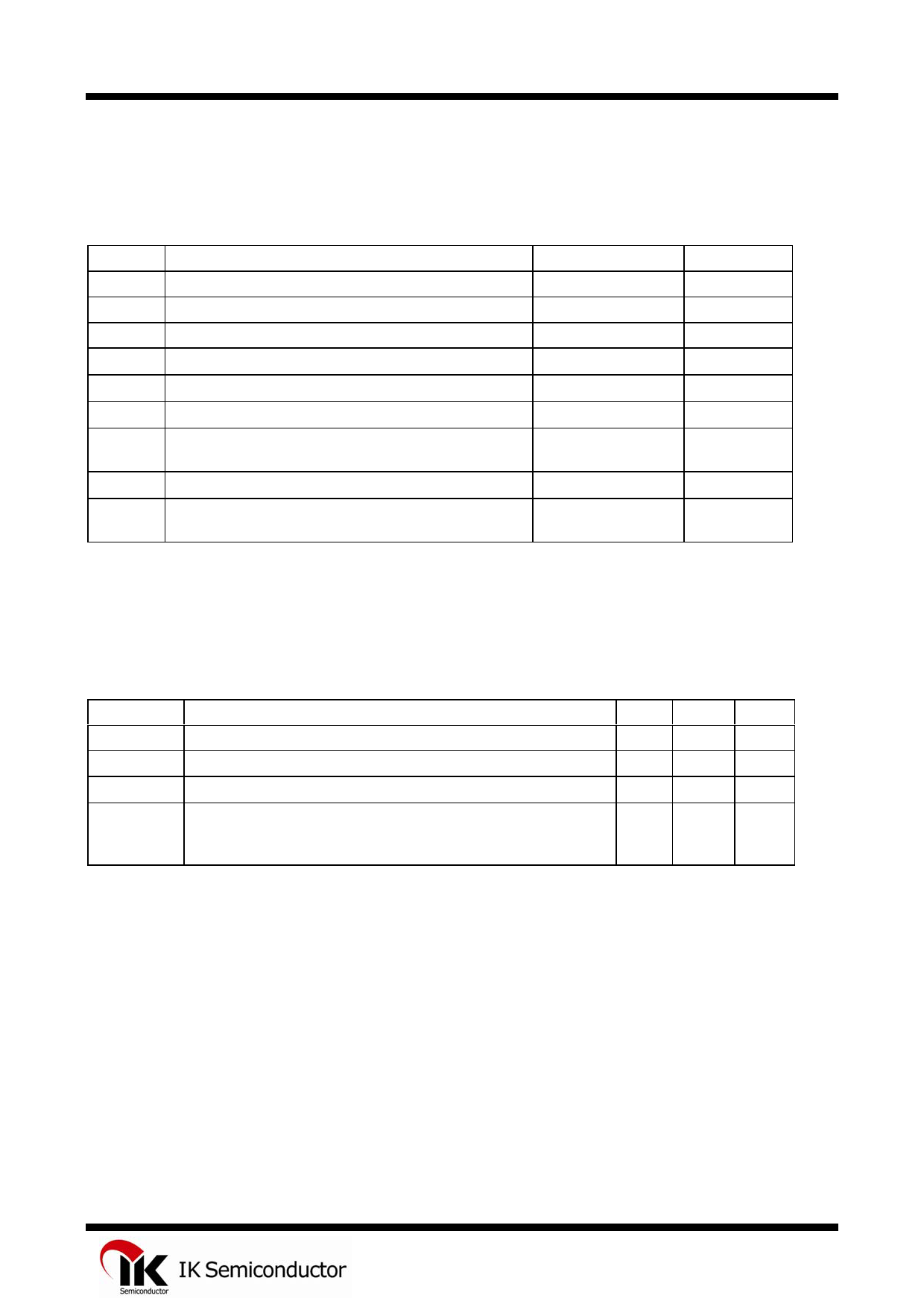
MAXIMUM RATINGS*
Symbol
Parameter
Value
Unit
VCC DC Supply Voltage (Referenced to GND)
-0.5 to +7.0
V
VIN DC Input Voltage (Referenced to GND)
-1.5 to VCC +1.5
V
VOUT DC Output Voltage (Referenced to GND)
-0.5 to VCC +0.5
V
IIN
DC Input Current, per Pin
±20
mA
IOUT DC Output Current, per Pin
±25
mA
ICC DC Supply Current, VCC and GND Pins
±50
mA
PD Power Dissipation in Still Air, Plastic DIP**
SOIC Package**
750
mW
500
Tstg Storage Temperature
-65 to +150
°C
TL Lead Temperature, 1 mm from Case for 10 Seconds
260
°C
(Plastic DIP or SOIC Package)
*Maximum Ratings are those values beyond which damage to the device may occur.
Functional operation should be restricted to the Recommended Operating Conditions.
**Derating - Plastic DIP: - 10 mW/°C from 65° to 125°C
SOIC Package: : - 7 mW/°C from 65° to 125°C
RECOMMENDED OPERATING CONDITIONS
Symbol
Parameter
VCC
VIN, VOUT
TA
DC Supply Voltage (Referenced to GND)
DC Input Voltage, Output Voltage (Referenced to GND)
Operating Temperature, All Package Types
tr, tf
Input Rise and Fall Time (Figure 1)
VCC =2.0 V
VCC =4.5 V
VCC =6.0 V
Min Max Unit
2.0 6.0
V
0
VCC
V
-55 +125 °C
0 1000 ns
0
500
0
400
This device contains protection circuitry to guard against damage due to high static voltages or electric fields.
However, precautions must be taken to avoid applications of any voltage higher than maximum rated voltages to this
high-impedance circuit. For proper operation, VIN and VOUT should be constrained to the range GND≤(VIN or
VOUT)≤VCC.
Unused inputs must always be tied to an appropriate logic voltage level (e.g., either GND or VCC). Unused
outputs must be left open.
2
Share Link: 