IDT74CBTLV16211 Просмотр технического описания (PDF) - Integrated Device Technology
Номер в каталоге
Компоненты Описание
Список матч
IDT74CBTLV16211 Datasheet PDF : 5 Pages
| |||
IDT74CBTLV16211
LOW-VOLTAGE 24-BIT BUS SWITCH
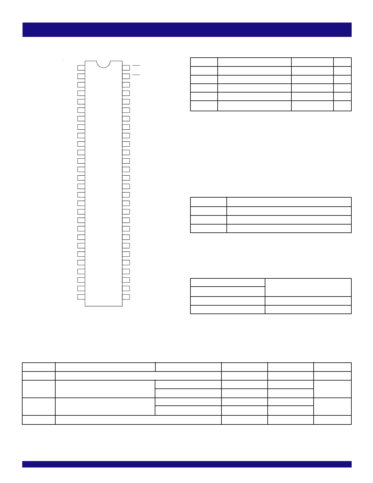
PIN CONFIGURATION
NC
1
56
1A1
2
55
1A2
3
54
1A3
4
53
1A4
5
52
1A5
6
51
1A6
7
50
GND
8
49
1A7
9
48
1A8
10
47
1A9
11
46
1A10
12
45
1A11
13
44
1A12
14
43
2A1
15
42
2A2
16
41
VCC
17
40
2A3
18
39
GND
19
38
2A4
20
37
2A5
21
36
2A6
22
35
2A7
23
34
2A8
24
33
2A9
25
32
2A10
26
31
2A11
27
30
2A12
28
29
1OE
2OE
1B1
1B2
1B3
1B4
1B5
GND
1B6
1B7
1B8
1B9
1B10
1B11
1B12
2B1
2B2
2B3
GND
2B4
2B5
2B6
2B7
2B8
2B9
2B10
2B11
2B12
SSOP/ TSSOP/ TVSOP
TOP VIEW
INDUSTRIAL TEMPERATURE RANGE
ABSOLUTE MAXIMUM RATINGS(1)
Symbol Description
Max.
Unit
VCC Supply Voltage Range
–0.5 to 4.6
V
VI
Input Voltage Range
Continuous Channel Current
–0.5 to 4.6
V
128
mA
IIK
Input Clamp Current, VI/O < 0
–50
mA
TSTG StorageTemperatureRange
–65 to +150
°C
NOTE:
1. Stresses greater than those listed under ABSOLUTE MAXIMUM RATINGS may cause
permanent damage to the device. This is a stress rating only and functional operation
of the device at these or any other conditions above those indicated in the operational
sections of this specification is not implied. Exposure to absolute maximum rating
conditions for extended periods may affect reliability.
PIN DESCRIPTION
Pin Names
Description
xOE
Output Enable (Active LOW)
xAx
Port A Inputs or Outputs
xBx
Port B Inputs or Outputs
FUNCTION TABLE(EACH 12-BIT BUS SWITCH)(1)
Input
OE
Operation
L
A-Port = B-Port
H
Disconnect
NOTE:
1. H = HIGH Voltage Level
L = LOW Voltage Level
OPERATING CHARACTERISTICS(1)
Symbol
Parameter
Test Conditions
Min.
VCC
Supply Voltage
2.3
VIH
High-Level Control Input Voltage
VCC = 2.3V to 2.7V
1.7
VCC = 2.7V to 3.6V
2
VIL
Low-Level Control Input Voltage
VCC = 2.3V to 2.7V
—
VCC = 2.7V to 3.6V
—
TA
Operating Free-Air Temperature
–40
NOTE:
1. All unused control inputs of the device must be held at VCC or GND to ensure proper device operation.
Max.
Unit
3.6
V
—
V
—
0.7
V
0.8
+85
°C
2
Share Link: 