IDT72V3622 Просмотр технического описания (PDF) - Integrated Device Technology
Номер в каталоге
Компоненты Описание
Список матч
IDT72V3622
Integrated Device Technology

IDT72V3622 Datasheet PDF : 29 Pages
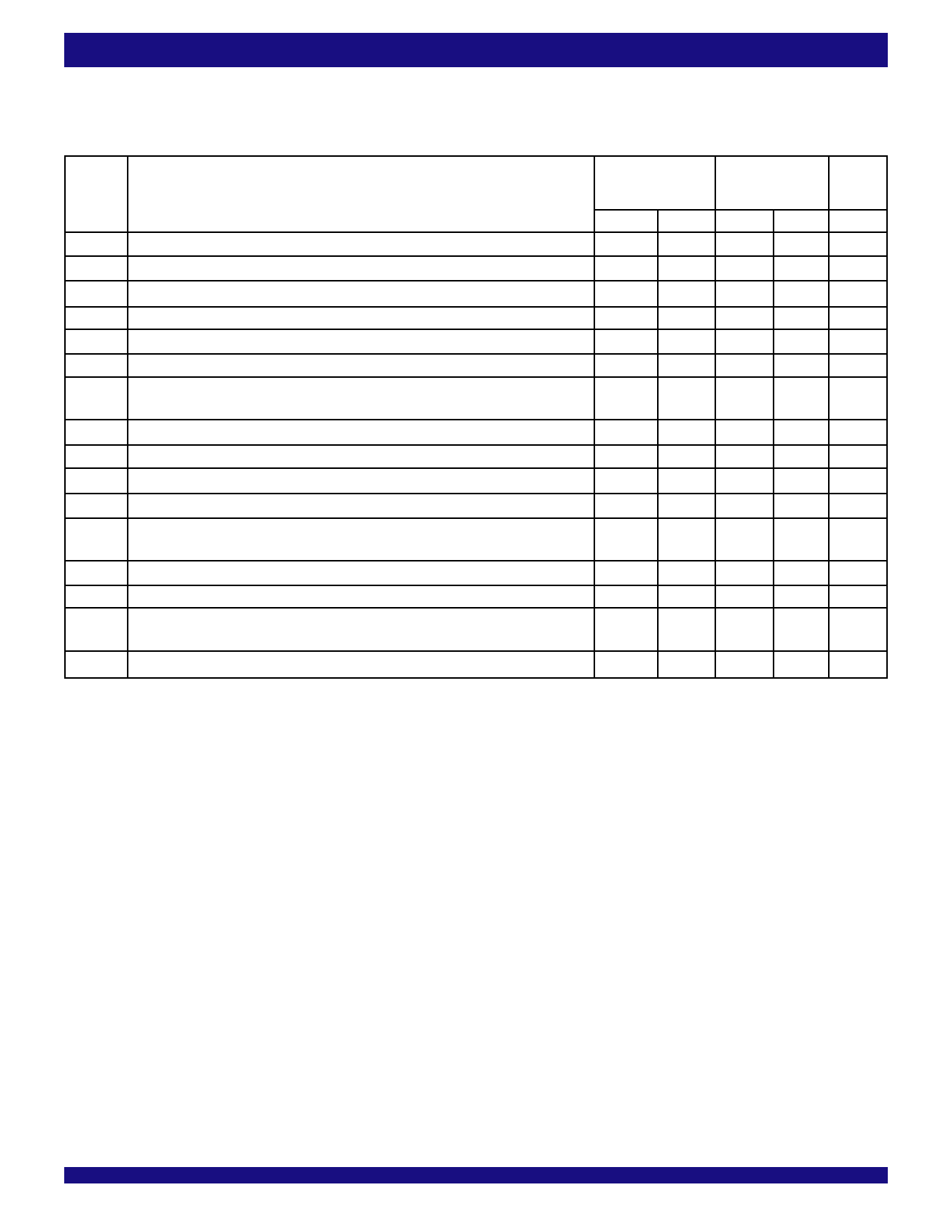
| |||
IDT72V3622/72V3632/72V3642 CMOS 3.3V SyncBiFIFOTM
256 x 36 x 2, 512 x 36 x 2, 1,024 x 36 x 2
COMMERCIAL TEMPERATURE RANGE
TIMING REQUIREMENTS OVER RECOMMENDED RANGES O. SUPPLY
VOLTAGE AND OPERATING .REE-AIR TEMPERATURE
Commercial: VCC=3.3V± 0.30V; for 10ns (100 MHz) operation, VCC=3.3V ±0.15V; TA = 0ο C to +70ο C; JEDEC JESD8-A compliant
Symbol
Parameter
IDT72V3622L10(1) IDT72V3622L15
IDT72V3632L10(1) IDT72V3632L15
IDT72V3642L10(1) IDT72V3642L15
Min. Max. Min. Max. Unit
fS
Clock Frequency, CLKA or CLKB
—
100
—
66.7 MHz
tCLK
Clock Cycle Time, CLKA or CLKB
10
—
15
—
ns
tCLKH
Pulse Duration, CLKA or CLKB HIGH
4.5
—
6
—
ns
tCLKL
Pulse Duration, CLKA and CLKB LOW
4.5
—
6
—
ns
tDS
tENS1
tENS2
tRSTS
tFSS
tFWS
Setup Time, A0-A35 before CLKA↑ and B0-B35 before CLKB↑
Setup Time CSA before CLKA↑; CSB before CLKB↑
Setup Time ENA, W/RA and MBA before CLKA↑; ENB, W/RB and MBB
before CLKB↑
Setup Time, RST1 or RST2 LOW before CLKA↑ or CLKB↑(2)
Setup Time, FS0 and FS1 before RST1 and RST2 HIGH
Setup Time, FWFT before CLKA↑
3
—
4
—
ns
4
—
4.5
—
ns
3
—
4.5
—
ns
5
—
5
—
ns
7.5
—
7.5
—
ns
0
—
0
—
ns
tDH
tENH
tRSTH
tFSH
tSKEW1(3)
tSKEW2(3,4)
Hold Time, A0-A35 after CLKA↑ and B0-B35 after CLKB↑
Hold Time, CSA, W/RA, ENA, and MBA after CLKA↑; CSB, W/RB, ENB, and
MBB after CLKB↑
Hold Time, RST1 or RST2 LOW after CLKA↑ or CLKB↑(2)
Hold Time, FS0 and FS1 after RST1 and RST2 HIGH
Skew Time, between CLKA↑ and CLKB↑ for EFA/ORA, EFB/ORB, FFA/IRA,
and FFB/IRB
Skew Time, between CLKA↑ and CLKB↑ for AEA, AEB, AFA, and AFB
0.5
—
1
—
ns
0.5
—
1
—
ns
4
—
4
—
ns
2
—
2
—
ns
7.5
—
7.5
—
ns
12
—
12
—
ns
NOTES:
1. For 10ns speed grade only: VCC = 3.3V +/- 0.15V, TA = 0° to +70°C; JEDEC JESD8-A compliant.
2. Requirement to count the clock edge as one of at least four needed to reset a FIFO.
3. Skew time is not a timing constraint for proper device operation and is only included to illustrate the timing relationship between CLKA cycle and CLKB cycle.
4. Design simulated, not tested.
5. Industrial temperature range is available by special order.
8
Share Link: