IDT72V3612L12PF Просмотр технического описания (PDF) - Integrated Device Technology
Номер в каталоге
Компоненты Описание
Список матч
IDT72V3612L12PF Datasheet PDF : 25 Pages
| |||
IDT72V3612 3.3V, CMOS SyncBiFIFOTM
64 x 36 x 2
COMMERCIAL TEMPERATURE RANGE
and has read access times as fast as 8ns. The FIFO operates in IDT Standard
mode. Two independent 64 x 36 dual-port SRAM FIFOs on board the chip
buffer data in opposite directions. Each FIFO has flags to indicate empty and
full conditions and two programmable flags (Almost-Full and Almost-Empty) to
indicate when a selected number of words is stored in memory. Communication
between each port can bypass the FIFOs via two 36-bit mailbox registers. Each
mailbox register has a flag to signal when new mail has been stored. Parity is
checked passively on each port and may be ignored if not desired. Parity
generation can be selected for data read from each port. Two or more devices
can be used in parallel to create wider data paths.
This device is a clocked FIFO, which means each port employs a
synchronous interface. All data transfers through a port are gated to the
LOW-to-HIGH transition of a port clock by enable signals. The clocks for
each port are independent of one another and can be asynchronous or
coincident. The enables for each port are arranged to provide a simple bi-
directional interface between microprocessors and/or buses with synchro-
nous control.
The Full Flag (FFA, FFB) and Almost-Full (AFA, AFB) flag of a FIFO
are two-stage synchronized to the port clock that writes data to its array.
The Empty Flag (EFA, EFB) and Almost-Empty (AEA, AEB) flag of a
FIFO are two stage synchronized to the port clock that reads data from
its array.
The IDT72V3612 is characterized for operation from 0°C to 70°C.
Industrial temperature range (–40°C to +85°C) is available by special order.
This device is fabricated using IDT's high speed, submicron CMOS
technology.
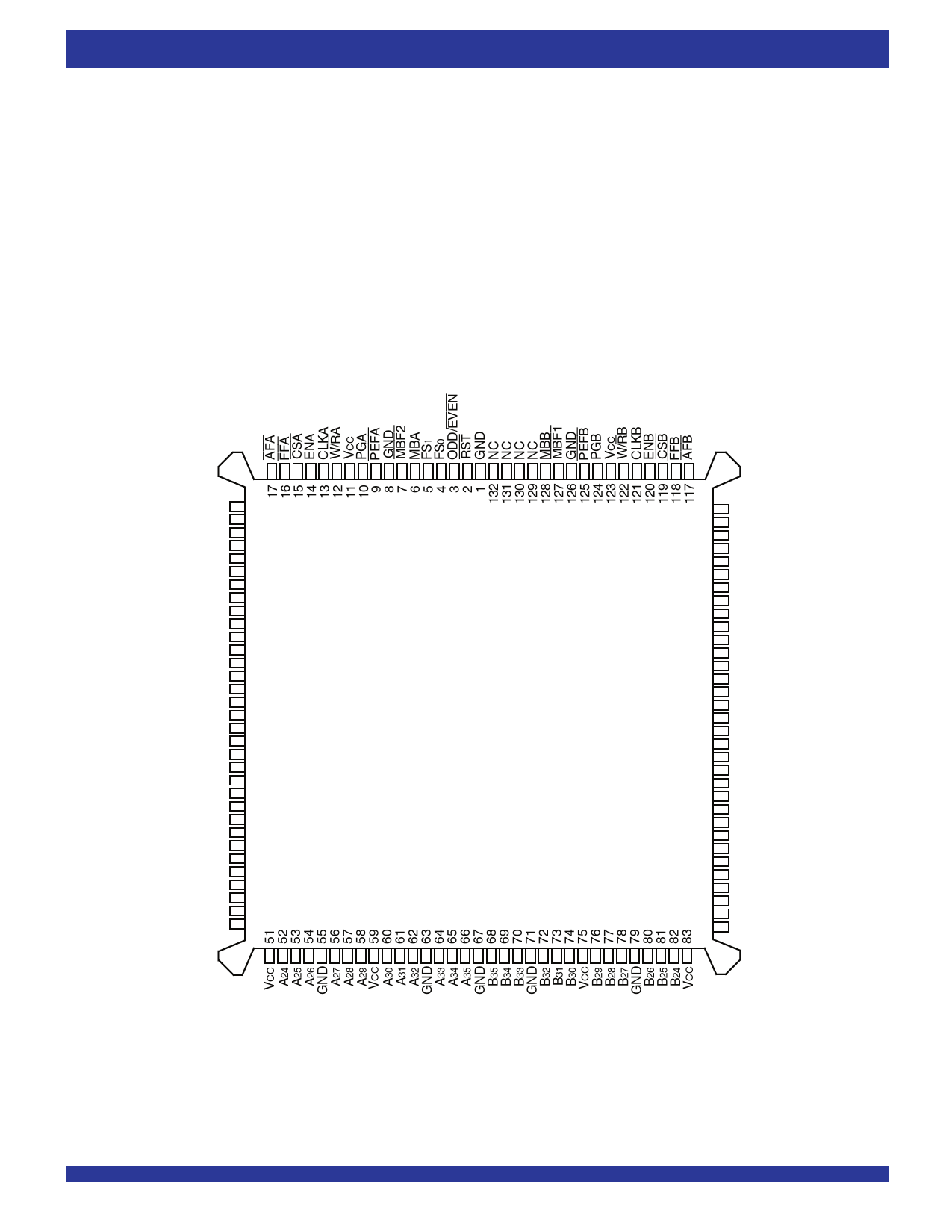
PIN CONFIGURATIONS
GND 18
AEA 19
EFA 20
A0 21
A1 22
*
A2 23
GND 24
A3 25
A4 26
A5 27
A6 28
VCC 29
A7 30
A8 31
A9 32
GND 33
A10 34
A11 35
VCC 36
A12 37
A13 38
A14 39
GND 40
A15 41
A16 42
A17 43
A18 44
A19 45
A20 46
GND 47
A21 48
A22 49
A23 50
*Electrical pin 1 in center of beveled edge. Pin 1 identifier in corner.
NOTES:
1. NC - No internal connection
2. Uses Yamaichi socket IC51-1324-828
PQFP(2) (PQ132-1, order code: PQF)
TOP VIEW
2
116 GND
115
114
AEB
EFB
113 B0
112 B1
111 B2
110 GND
109 B3
108 B4
107 B5
106 B6
105 VCC
104 B7
103 B8
102 B9
101 GND
100 B10
99 B11
98 VCC
97 B12
96 B13
95 B14
94 GND
93 B15
92 B16
91 B17
90 B18
89 B19
88 B20
87 GND
86 B21
85 B22
84 B23
4659 drw 02
Share Link: 