IDT723644 Просмотр технического описания (PDF) - Integrated Device Technology
Номер в каталоге
Компоненты Описание
Список матч
IDT723644
Integrated Device Technology

IDT723644 Datasheet PDF : 35 Pages
| |||
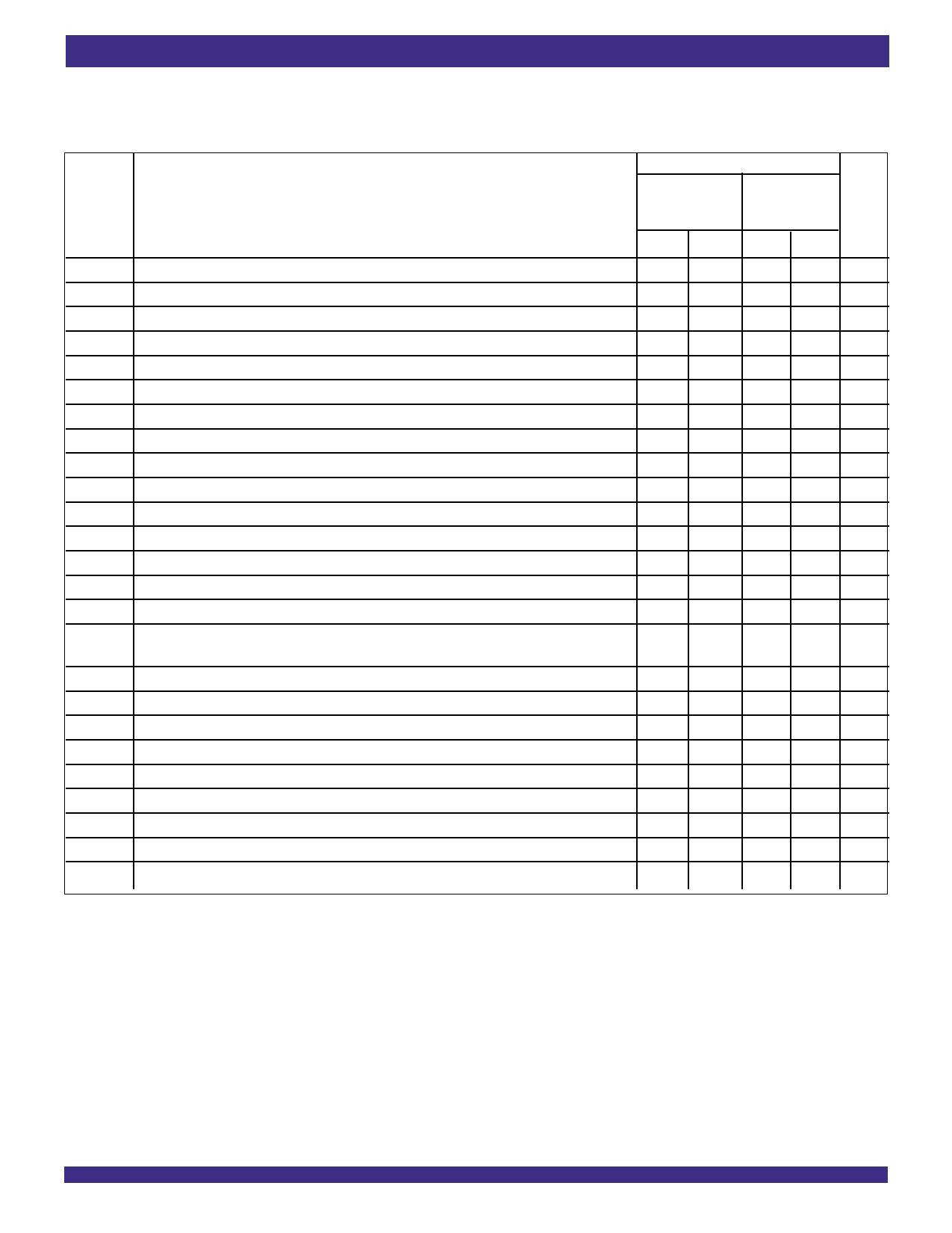
IDT723624/723634/723644 CMOS SyncBiFIFO™ WITH BUS-MATCHING
256 x 36 x 2, 512 x 36 x 2, 1,024 x 36 x 2
COMMERCIAL TEMPERATURE RANGE
TIMING REQUIREMENTS OVER RECOMMENDED RANGES O. SUPPLY
VOLTAGE AND OPERATING .REE-AIR TEMPERATURE
(Commercial: VCC = 5V ± 10%, TA = 0°C to +70°C)
Commercial
IDT723624L12 IDT723624L15
IDT723634L12 IDT723634L15
IDT723644L12 IDT723644L15
Symbol
Parameter
Min. Max. Min. Max. Unit
fS
Clock Frequency, CLKA or CLKB
—
83 — 66.7 MHz
tCLK
Clock Cycle Time, CLKA or CLKB
12
— 15 — ns
tCLKH
Pulse Duration, CLKA or CLKB HIGH
5
—6
—
ns
tCLKL
Pulse Duration, CLKA and CLKB LOW
5
—6
—
ns
tDS
Setup Time, A0-A35 before CLKA↑ and B0-B35 before CLKB↑
tENS1
Setup Time, CSA and W/RA before CLKA↑; CSB and W/RB before CLKB↑
3
—4
—
ns
4
— 4.5 — ns
tENS2
Setup Time ENA and MBA before CLKA↑; ENB and MBB before CLKB↑
3
— 4.5 — ns
tRSTS
tFSS
Setup Time, MRS1, MRS2, PRS1, or PRS2 LOW before CLKA↑ or CLKB↑(2)
Setup Time, FS0 and FS1 before MRS1 and MRS2 HIGH
5
—5
—
ns
7.5
— 7.5 —
ns
tBES
Setup Time, BE/FWFT before MRS1 and MRS2 HIGH
7.5
— 7.5 —
ns
tSPMS Setup Time, SPM before MRS1 and MRS2 HIGH
7.5
— 7.5 —
ns
tSDS
tSENS
Setup Time, FS0/SD before CLKA↑
Setup Time, FS1/SEN before CLKA↑
3
—4
—
ns
3
—4
—
ns
tFWS
Setup Time, BE/FWFT before CLKA↑
0
—0
—
ns
tDH
Hold Time, A0-A35 after CLKA↑ and B0-B35 after CLKB↑
tENH
Hold Time, CSA, W/RA, ENA, and MBA after CLKA↑; CSB, W/RB, ENB, and MBB
after CLKB↑
0.5
—1
—
ns
0.5
—1
—
ns
tRSTH
tFSH
Hold Time, MRS1, MRS2, PRS1 or PRS2 LOW after CLKA↑ or CLKB↑(2)
Hold Time, FS0 and FS1 after MRS1 and MRS2 HIGH
4
—4
—
ns
2
—2
—
ns
tBEH
Hold Time, BE/FWFT after MRS1 and MRS2 HIGH
2
—2
—
ns
tSPMH Hold Time, SPM after MRS1 and MRS2 HIGH
2
—2
—
ns
tSDH
tSENH
Hold Time, FS0/SD after CLKA↑
Hold Time, FS1/SEN HIGH after CLKA↑
0.5
—1
—
ns
0.5
—1
—
ns
tSPH
Hold Time, FS1/SEN HIGH after MRS1 and MRS2 HIGH
2
—2
—
ns
tSKEW1(3) Skew Time between CLKA↑ and CLKB↑ for EFA/ORA, EFB/ORB, FFA/IRA, and FFB/IRB 5
tSKEW2(3,4) Skew Time between CLKA↑ and CLKB↑ for AEA, AEB, AFA, and AFB
12
— 7.5 — ns
— 12 — ns
NOTES:
1. Industrial temperature range is available by special order.
2. Requirement to count the clock edge as one of at least four needed to reset a FIFO.
3. Skew time is not a timing constraint for proper device operation and is only included to illustrate the timing relationship between CLKA cycle and CLKB cycle.
4. Design simulated, not tested.
8
Share Link: