IDT7134 Просмотр технического описания (PDF) - Integrated Device Technology
Номер в каталоге
Компоненты Описание
Список матч
IDT7134 Datasheet PDF : 9 Pages
| |||
IDT7134SA/LA
HIGH-SPEED 4K x 8 DUAL-PORT STATIC RAM
MILITARY AND COMMERCIAL TEMPERATURE RANGES
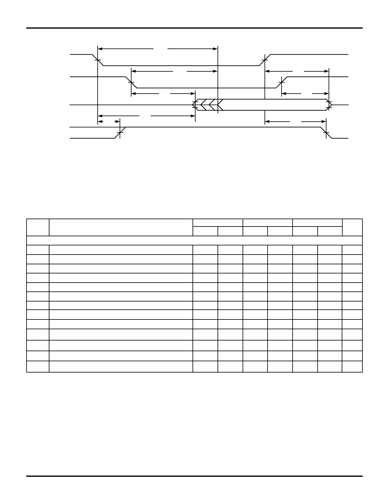
TIMING WAVEFORM OF READ CYCLE NO. 2, EITHER SIDE(1, 3)
tACE
CE
tAOE(4)
OE
DATAOUT
tLZ(1)
ICC
CURRENT
ISB
tLZ(1)
tPU
50%
NOTES:
1. Timing depends on which signal is asserted last, OE or CE.
2. Timing depends on which signal is de-asserted first, OE or CE.
3. R/W = VIH.
4. Start of valid data depends on which timing becomes effective , tAOE, tACE or tAA
5. tAA for RAM Address Access and tSAA for Semaphore Address Access.
tHZ(2)
tHZ(2)
VALID DATA (4)
tPD
50%
2720 drw 09
AC ELECTRICAL CHARACTERISTICS OVER THE
OPERATING TEMPERATURE AND SUPPLY VOLTAGE(6)
7134X20(5)
Symbol
Parameter
Min. Max.
WRITE CYCLE
tWC
Write Cycle Time
20
—
tEW
Chip Enable to End-of-Write
15
—
tAW
Address Valid to End-of-Write
15
—
tAS
Address Set-up Time
0
—
tWP
Write Pulse Width
15
—
tWR
Write RecoveryTime
0
—
tDW
Data Valid to End-of-Write
15
—
tHZ
Output High-Z Time(1, 2)
—
15
tDH
Data Hold Time(3)
0
—
tWZ
Write Enabled to Output in High-Z(1, 2)
—
15
tOW
Output Active from End-of-Write(1, 2, 3)
3
—
tWDD
Write Pulse to Data Delay(4)
—
40
tDDD Write Data Valid to Read Data Delay(4, 7)
—
30
7134X25
Min. Max.
25
—
20
—
20
—
0
—
20
—
0
—
15
—
—
15
0
—
—
15
3
—
—
50
—
30
7134X35
Min. Max. Unit
35
—
ns
30
—
ns
30
—
ns
0
—
ns
25
—
ns
0
—
ns
20
—
ns
—
20
ns
3
—
ns
—
20
ns
3
—
ns
—
60
ns
—
35
ns
NOTES:
2720 tbl 10
1. Transition is measured ±500mV from Low or High-impedance voltage with Output Test Load (Figure 2).
2. This parameter is guaranteed by device characterization, but is not production tested.
3. The specification for tDH must be met by the device supplying write data to the RAM under all operating conditions. Although tDH and tOW values will vary
over voltage and temperature, the actual tDH will always be smaller than the actual tOW.
4. Port-to-port delay through RAM cells from writing port to reading port, refer to “Timing Waveform of Write with Port-to-Port Read”.
5. (Commercial only), 0°C to +70°C temperature range .
6. “X” in part number indicates power rating (SA or LA).
7. tDDD = 35ns for military temperature range.
6.04
6
Share Link: 