IDT71128S12Y Просмотр технического описания (PDF) - Integrated Device Technology
Номер в каталоге
Компоненты Описание
Список матч
IDT71128S12Y Datasheet PDF : 8 Pages
| |||
IDT71128 CMOS Static RAM
1 Meg (256K x 4-bit) Revolutionary Pinout
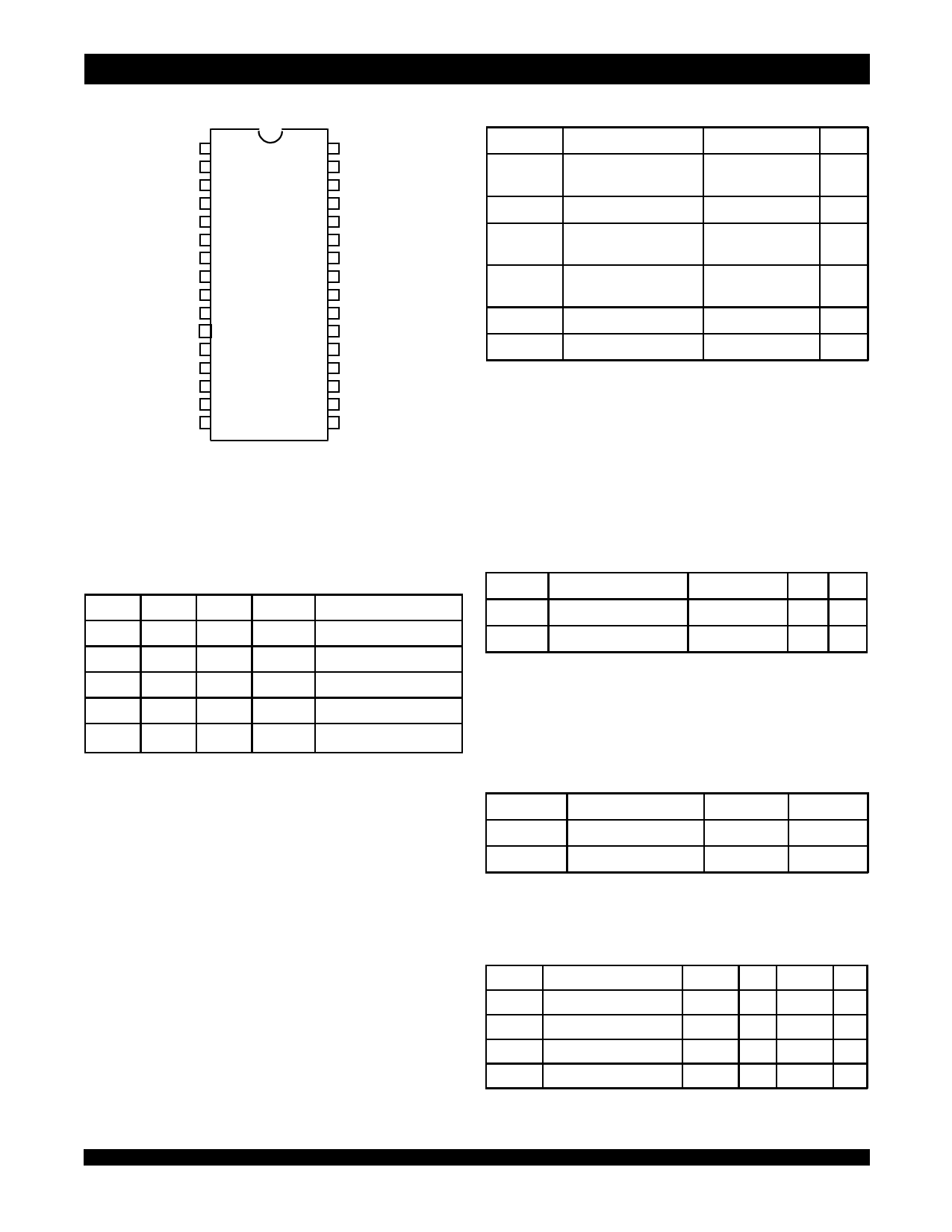
Pin Configuration
NC
A0
A1
A2
A3
CS
I/O0
VCC
GND
I/O1
WE
A4
A5
A6
A7
NC
1
32
2
31
3
30
4
29
5
28
6 SO32-3 27
7
26
8
25
9
24
10
23
11
22
12
21
13
20
14
19
15
18
16
17
A17
A16
A15
A14
A13
OE
I/O3
GND
VCC
I/O2
A12
A11
A10
A9
A8
NC
SOJ
3483 drw 02
Top View
Commercial and Industrial Temperature Ranges
Absolute Maximum Ratings(1)
Symbol
VTERM(2)
Rating
Terminal Voltage with
Respect to GND
Value
Unit
-0.5 to +7.0(2)
V
TA
Operating Temperature
0 to +70
oC
TBIAS
Temperature
Under Bias
-55 to +125
oC
TSTG
Storage
Temperature
-55 to +125
oC
PT
Power Dissipation
1.25
W
IOUT
DC Output Current
50
mA
NOTES:
3483 tbl 02
1. StressesgreaterthanthoselistedunderABSOLUTEMAXIMUMRATINGSmaycause
permanent damage to the device. This is a stress rating only and functional operation
of the device at these or any other conditions above those indicated in the operational
sections of this specification is not implied. Exposure to absolute maximum rating
conditions for extended periods may affect reliability.
2. VTERMmust not exceed Vcc + 0.5V.
Truth Table(1,2)
CS
OE
WE
I/O
Function
L
L
H
DATAOUT Read Data
L
X
L
DATAIN Write Data
L
H
H
High-Z Output Disabled
H
X
X
High-Z Deselected - Standby (ISB)
VHC(3)
X
X
High-Z Deselected - Standby (ISB1)
NOTES:
1. H = VIH, L = VIL, x = Don't care.
2. VLC = 0.2V, VHC = VCC -0.2V.
3. Other inputs ≥VHC or ≤VLC.
3483 tbl 01
Capacitance
(TA = +25°C, f = 1.0MHz, SOJ package)
Symbol
Parameter(1)
Conditions Max. Unit
CIN Input Capacitance
VIN = 3dV
8 pF
CI/O I/O Capacitance
VOUT = 3dV
8 pF
NOTE:
3483 tbl 03
1. This parameter is guaranteed by device characterization, but is not production tested.
Recommended Operating
Temperature and Supply Voltage
Grade
Temperature
GND
VCC
Commercial
0°C to +70°C
0V
5.0V ± 10%
Industrial
–40°C to +85°C
0V
5.0V ± 10%
3483 tbl 04
Recommended DC Operating
Conditions
Symbol
Parameter
Min. Typ. Max. Unit
VCC Supply Voltage
4.5
5.0
5.5
V
GND Ground
0
0
0
V
VIH Input High Voltage
2.2
____ VCC +0.5 V
VIL Input Low Voltage
-0.5(1)
____
0.8
V
NOTE:
1. VIL (min.) = –1.5V for pulse width less than 10ns, once per cycle.
3483 tbl 05
6.422
Share Link: 