IDT71024S Просмотр технического описания (PDF) - Integrated Device Technology
Номер в каталоге
Компоненты Описание
Список матч
IDT71024S Datasheet PDF : 8 Pages
| |||
IDT71024 CMOS Static RAM
1 Meg (128K x 8-Bit)
Commercial and Industrial Temperature Ranges
DC Electrical Characteristics
(VCC = 5.0V ± 10%, Commercial and Industrial Temperature Ranges)
IDT71024
Symbol
|ILI|
|ILO|
VOL
VOH
Parameter
Input Leakage Current
Output Leakage Current
Output Low Voltage
Output High Voltage
Test Condition
VCC = Max., VIN = GND to VCC
VCC = Max., CS1 = VIH, VOUT = GND to VCC
IOL = 8mA, VCC = Min.
IOH = –4mA, VCC = Min.
Min.
___
___
___
2.4
Max. Unit
5
µA
5
µA
0.4
V
___
V
2964 tbl 06
DC Electrical Characteristics(1)
(VCC = 5.0V ± 10%, VLC = 0.2V, VHC = VCC – 0.2V)
Symbol
ICC
ISB
ISB1
Parameters
Dynamic Operating Current,
CS2 ≥ VIH and CS1 ≤ VIL, Outputs Open,
VCC = Max., f = fMAX(2)
Standby Power Supply Current (TTL Level)
CS1 ≥ VIH or CS2 ≤ VIL, Outputs Open,
VCC = Max., f=fMAX(2)
Full Standby Power Supply Current
(CMOS Level), CS1 ≥ VHC or
CS2 ≤ VLC, Outputs Open,
VCC = Max., f = 0(2), VIN ≤ VLC or VIN ≥ VHC
71024S12
Com'l.
Ind.
160
160
40
40
10
10
NOTES:
1. All values are maximum guaranteed values.
2. fMAX = 1/tRC (all address inputs are cycling at fMAX); f = 0 means no address
input lines are changing.
71024S15
Com'l.
Ind.
155
155
71024S20
Com'l.
Ind.
140
140
40
40
40
40
10
10
10
10
Unit
mA
mA
mA
2964 tbl 07
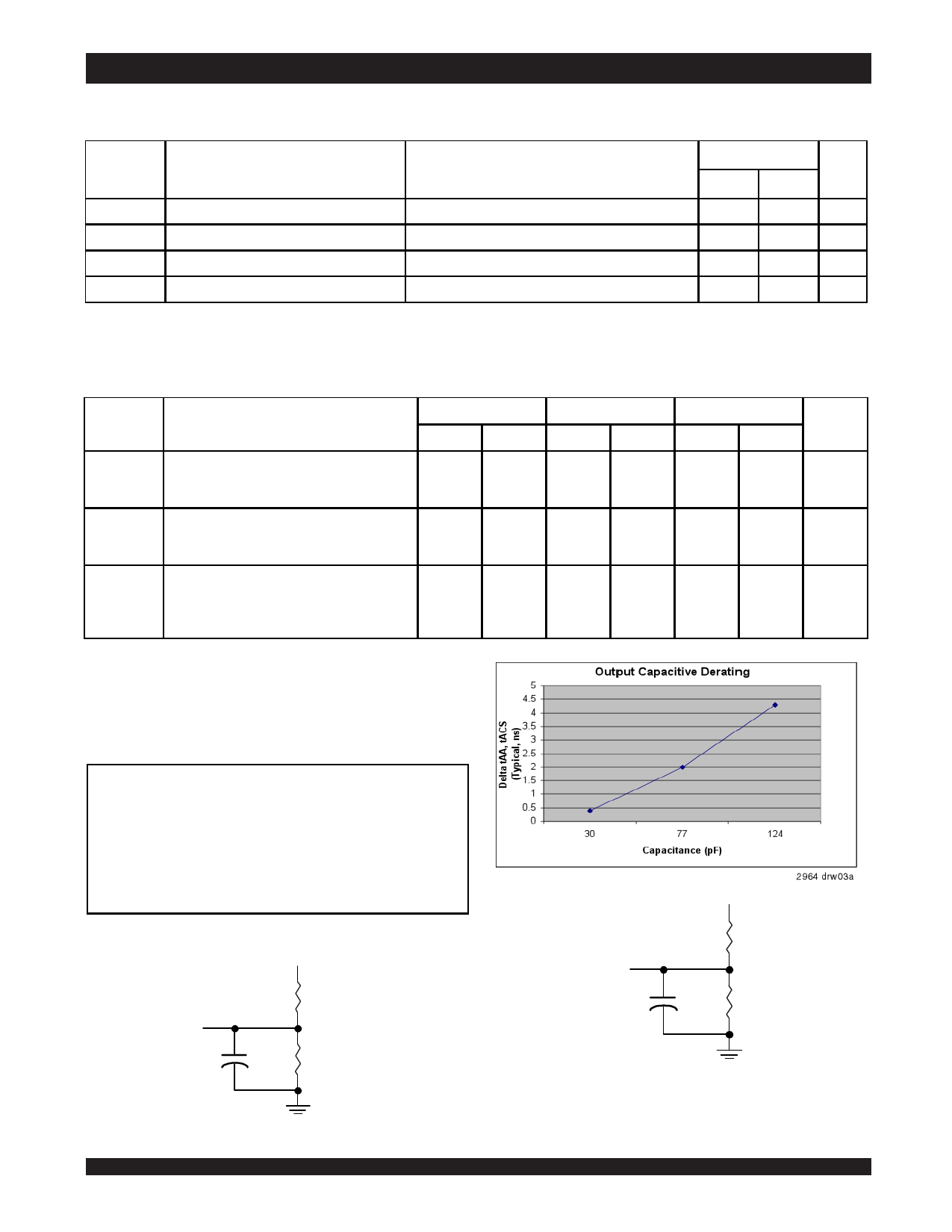
AC Test Conditions
Input Pulse Levels
GND to 3.0V
Input Rise/Fall Times
3ns
Input Timing Reference Levels
1.5V
Output Reference Levels
1.5V
AC Test Load
See Figures 1 and 2
2964 tbl 08
5V
DATA OUT
30pF
480Ω
255Ω
2964 drw 03
Figure 1. AC Test Load
6.432
DATA OUT
5pF*
5V
480Ω
255Ω
2964 drw 04
*Including jig and scope capacitance.
Figure 2. AC Test Load
(for tCLZ, tOLZ, tCHZ, tOHZ, tOW, and tWHZ)
Share Link: 