FCT162240AT(2002) Просмотр технического описания (PDF) - Integrated Device Technology
Номер в каталоге
Компоненты Описание
Список матч
FCT162240AT Datasheet PDF : 6 Pages
| |||
IDT74FCT162240AT/CT
FAST CMOS 16-BIT BUFFER/LINE DRIVER
INDUSTRIAL TEMPERATURE RANGE
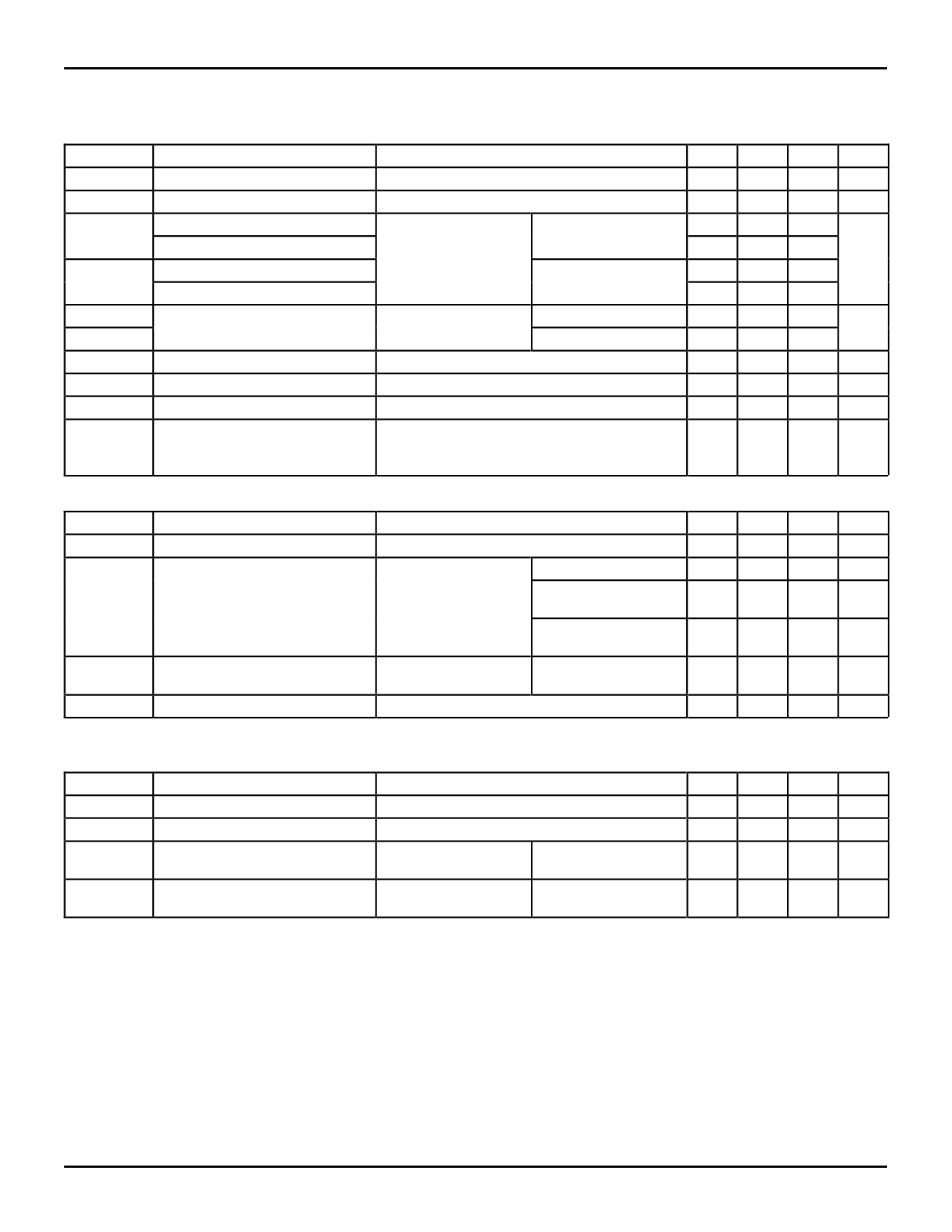
POWER SUPPLY CHARACTERISTICS
Symbol
Parameter
Test Conditions(1)
Min.
∆ICC
Quiescent Power Supply Current
VCC = Max.
—
TTL Inputs HIGH
VIN = 3.4V(3)
ICCD
Dynamic Power Supply
VCC = Max.
VIN = VCC
—
Current(4)
Outputs Open
xOE = GND
VIN = GND
One Input Toggling
50% Duty Cycle
IC
Total Power Supply Current(6)
VCC = Max.
Outputs Open
fi = 10MHz
VIN = VCC
—
VIN = GND
50% Duty Cycle
VIN = 3.4V
—
xOE = GND
VIN = GND
One Bit Toggling
VCC = Max.
Outputs Open
fi = 2.5MHz
VIN = VCC
—
VIN = GND
50% Duty Cycle
VIN = 3.4V
—
xOE = GND
VIN = GND
Sixteen Bits Toggling
NOTES:
1. For conditions shown as Min. or Max., use appropriate value specified under Electrical Characteristics for the applicable device type.
2. Typical values are at VCC = 5.0V, +25°C ambient.
3. Per TTL driven input; (VIN = 3.4V). All other inputs at VCC or GND.
4. This parameter is not directly testable, but is derived for use in Total Power Supply Calculations.
5. Values for these conditions are examples of the ICC formula. These limits are guaranteed but not tested.
6. IC = IQUIESCENT + IINPUTS + IDYNAMIC
IC = ICC + ∆ICC DHNT + ICCD (fCPNCP/2 + fiNi)
ICC = Quiescent Current (ICCL, ICCH and ICCZ)
∆ICC = Power Supply Current for a TTL High Input (VIN = 3.4V)
DH = Duty Cycle for TTL Inputs High
NT = Number of TTL Inputs at DH
ICCD = Dynamic Current caused by an Input Transition Pair (HLH or LHL)
fCP = Clock Frequency for Register Devices (Zero for Non-Register Devices)
NCP = Number of Clock Inputs at fCP
fi = Input Frequency
Ni = Number of Inputs at fi
Typ.(2)
0.5
60
0.6
0.9
2.4
6.4
Max.
1.5
100
1.5
2.3
4.5(5)
16.5(5)
Unit
mA
µA/
MHz
mA
SWITCHING CHARACTERISTICS OVER OPERATING RANGE
Symbol
tPLH
tPHL
tPZH
tPZL
tPHZ
tPLZ
tSK(o)
Parameter
Propagation Delay
xAx to xYx
Output Enable Time
Output Disable Time
Output Skew(3)
Condition(1)
CL = 50pF
RL = 500Ω
FCT162240AT
Min.(2)
Max.
1.5
4.8
1.5
6.2
1.5
5.6
—
0.5
FCT162240CT
Min.(2)
Max.
Unit
1.5
3.4
ns
1.5
4.4
ns
1.5
4.1
ns
—
0.5
ns
NOTES:
1. See test circuit and waveforms.
2. Minimum limits are guaranteed but not tested on Propagation Delays.
3. Skew between any two outputs of the same package switching in the same direction. This parameter is guaranteed by design.
4
Share Link: 