IDT29FCT2520BT Просмотр технического описания (PDF) - Integrated Device Technology
Номер в каталоге
Компоненты Описание
Список матч
IDT29FCT2520BT Datasheet PDF : 7 Pages
| |||
IDT29FCT520AT/BT/CT/DT, 521AT/BT/CT/DT
MULTILEVEL PIPELINE REGISTERS
MILITARY AND COMMERCIAL TEMPERATURE RANGES
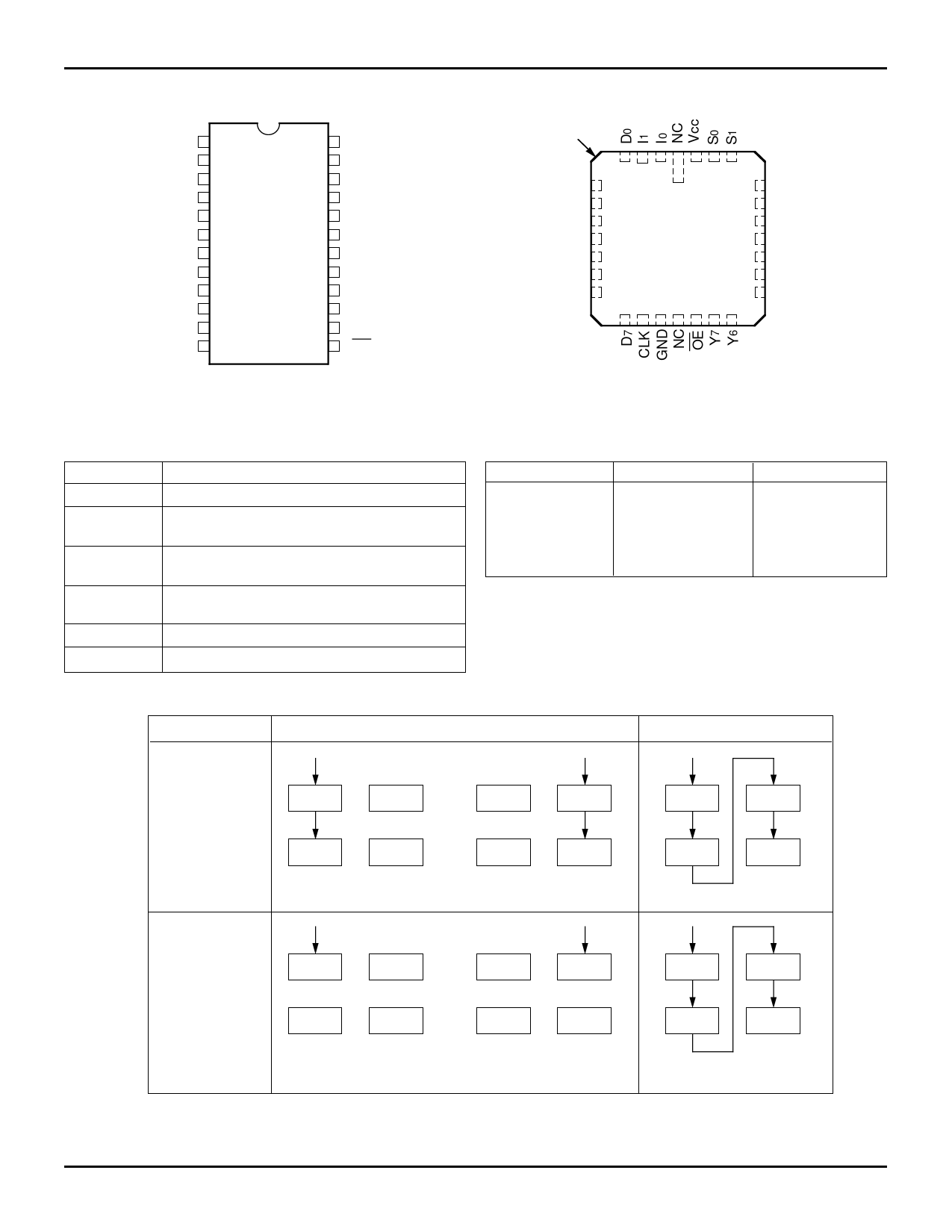
PIN CONFIGURATIONS
I0 1
24 Vcc
I1 2
23 S 0
D0 3
22 S 1
D 1 4 P24-1 21 Y 0
D 2 5 D24-1 20
D3
D4
SO24-2
6 SO24-7 19
7 SO24-8* 18
Y1
Y2
Y3
D5 8
&
17 Y 4
D 6 9 E24-1 16 Y 5
D 7 10
15 Y 6
CLK 11
14 Y 7
GND 12
13 OE
2619 drw 02
DIP/SOIC/SSOP/QSOP/CERPACK
*FCT520 only
TOP VIEW
INDEX
4 3 2 28 27 26
D1 5
D2 6
1
25 Y0
24 Y1
D3 7
23 Y2
NC 8
L28-1
22 NC
D4 9
21 Y3
D5 10
20 Y4
D6 11
19 Y5
12 13 14 15 16 17 18
2619 drw 03
LCC
TOP VIEW
DEFINITION OF FUNCTIONAL TERMS
Pin Names
Description
Dn
Register input Port.
CLK
Clock input. Enter data into registers on LOW-
to-HIGH transitions.
I0, I1
Instruction inputs. See Figure 1 and
in-
struction Control Tables.
S0, S1
OE
Multiplexer select. Inputs either register A1, A2,
B1 or B2 data to be available at the output port.
Output enable for 3-state output port.
Yn
Register output port.
REGISTER SELECTION
S1
S0
0
0
0
1
1
0
1
1
Register
B2
B1
A2
A1
2619 tbl 02
2619 tbl 01
DUAL 2-LEVEL
SINGLE 4-LEVEL
IDT29FCT520T
A1
B1
A2
B2
I=2
A1
B1
A2
B2
I=1
A1
B1
A2
B2
I=0
IDT29FCT521T
NOTE:
1. I = 3 for hold.
A1
B1
A2
B2
I=2
A1
B1
A2
B2
I=1
Figure 1. Data Loading in 2-Level Operation
6.2
A1
B1
A2
B2
I=0
2619 drw 04
2
Share Link: 