ICS9250-32 Просмотр технического описания (PDF) - Integrated Circuit Systems
Номер в каталоге
Компоненты Описание
Список матч
ICS9250-32 Datasheet PDF : 11 Pages
| |||
ICS9250-32
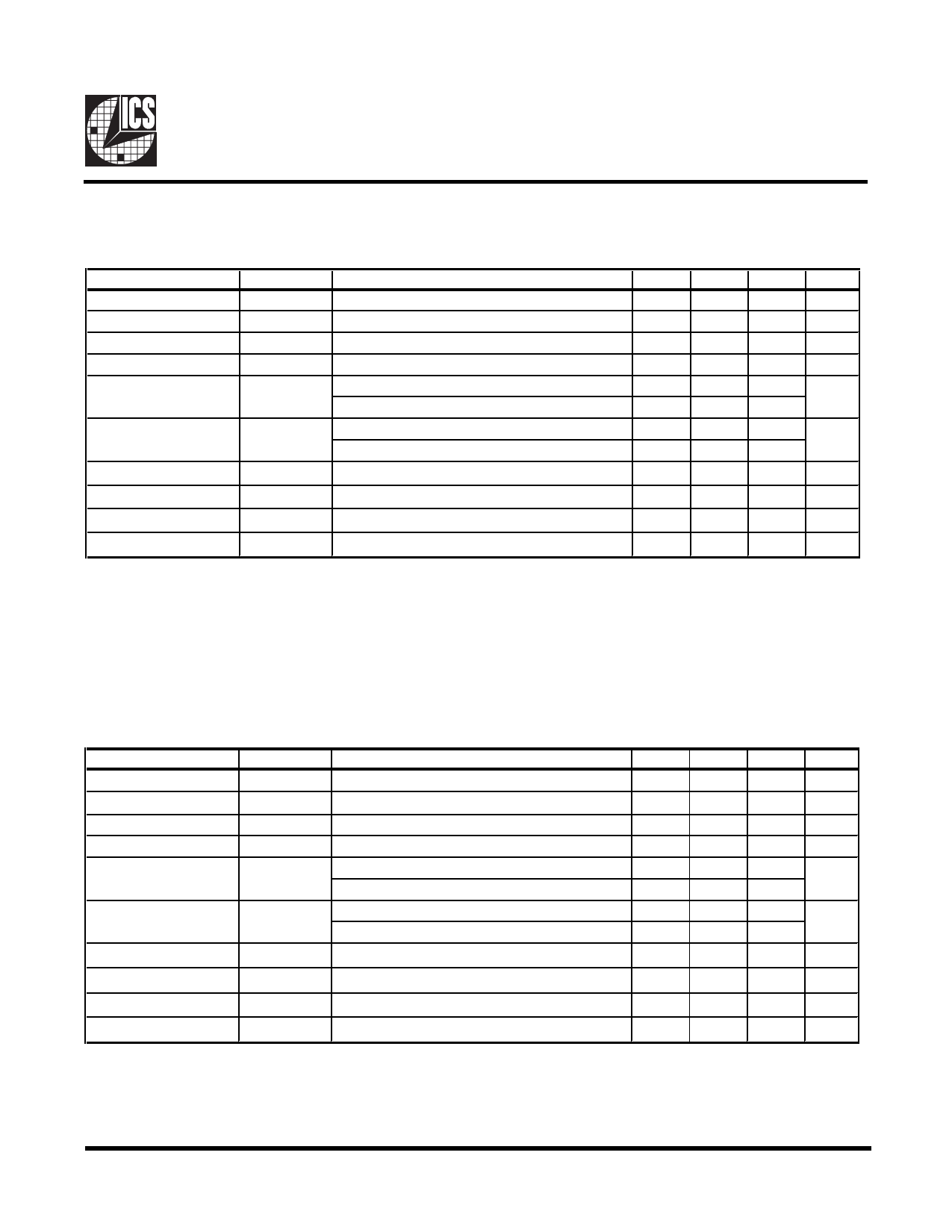
Electrical Characteristics - 2V48M
TA = 0 - 70C; VDDL = 2.5 V +/-5%; CL = 10-20 pF (unless otherwise specified)
PARAMETER
SYMBOL
CONDITIONS
MIN TYP MAX UNITS
Output Impedance1
Output Impedance1
Output High Voltage
Output Low Voltage
RDSP5
RDSN5
VOH5
VOL5
VO = VDD*(0.5)
VO = VDD*(0.5)
IOH = -1 mA
IOL = 1 mA
9.5
45
Ω
9.5
45
Ω
2
2.5
V
0.007 0.4
V
Output High Current
IOH5
VOH @ MIN = 1.0 V
VOH @ MAX = 2.375 V
-93
-27 mA
-27 -11
Output Low Current
Rise Time1
IOL5
VOL @ MIN = 1.2 V
VOL @ MAX = 0.3 V
tr5
VOL = 0.4 V, VOH = 2.0 V
27
81
mA
27
30
0.4 0.7 1.6 ns
Fall Time1
tf5
VOH = 2.0 V, VOL = 0.4 V
0.4 0.7 1.6 ns
Duty Cycle1
dt5
VT = 1.25 V
45
53
55
%
Jitter, Cycle-to-cycle1
tjcyc-cyc5 VT = 1.25 V
180 250 ps
1Guaranteed by design, not 100% tested in production.
AC timing of the trise & tfall is controlled by pre-driver circuit which allows lower impedance output to stay in the middle of
transition time target.
Electrical Characteristics - 3V48M
TA = 0 - 70C; VDD = 3.3 V +/-5%; CL = 10-15 pF (unless otherwise specified)
PARAMETER
Output Impedance1
Output Impedance1
Output High Voltage
Output Low Voltage
Output High Current
Output Low Current
Rise Time1
Fall Time1
Duty Cycle1
Jitter, Cycle-to-cycle1
SYMBOL
RDSP5
RDSN5
VOH5
VOL5
IOH5
IOL5
tr5
tf5
dt5
tjcyc-cyc5
CONDITIONS
VO = VDD*(0.5)
VO = VDD*(0.5)
IOH = -1 mA
IOL = 1 mA
VOH @ MIN = 2.0 V
VOH @ MAX = 3.135 V
VOL @ MIN = 1.0 V
VOL @ MAX = 0.4 V
VOL = 0.4 V, VOH = 2.4 V
VOH = 2.4 V, VOL = 0.4 V
VT = 1.5 V
VT = 1.5 V, CPU=66,100,133 MHz
MIN TYP MAX UNITS
16
24
60
Ω
16
60
Ω
2.4 3.3
V
0.014 0.4 V
-65
-27 mA
-23
-8
29
65
mA
21
27
0.5 1.2
2
ns
0.5 1.6
2
ns
45
54
55
%
290 500 ps
1Guaranteed by design, not 100% tested in production.
AC timing of the trise & tfall is controlled by pre-driver circuit which allows lower impedance output to stay in the middle of
transition time target.
Third party brands and names are the property of their respective owners.
7
Share Link: 