ICS9214 Просмотр технического описания (PDF) - Integrated Circuit Systems
Номер в каталоге
Компоненты Описание
Список матч
ICS9214 Datasheet PDF : 16 Pages
| |||
Integrated
Circuit
Systems, Inc.
ICS9214
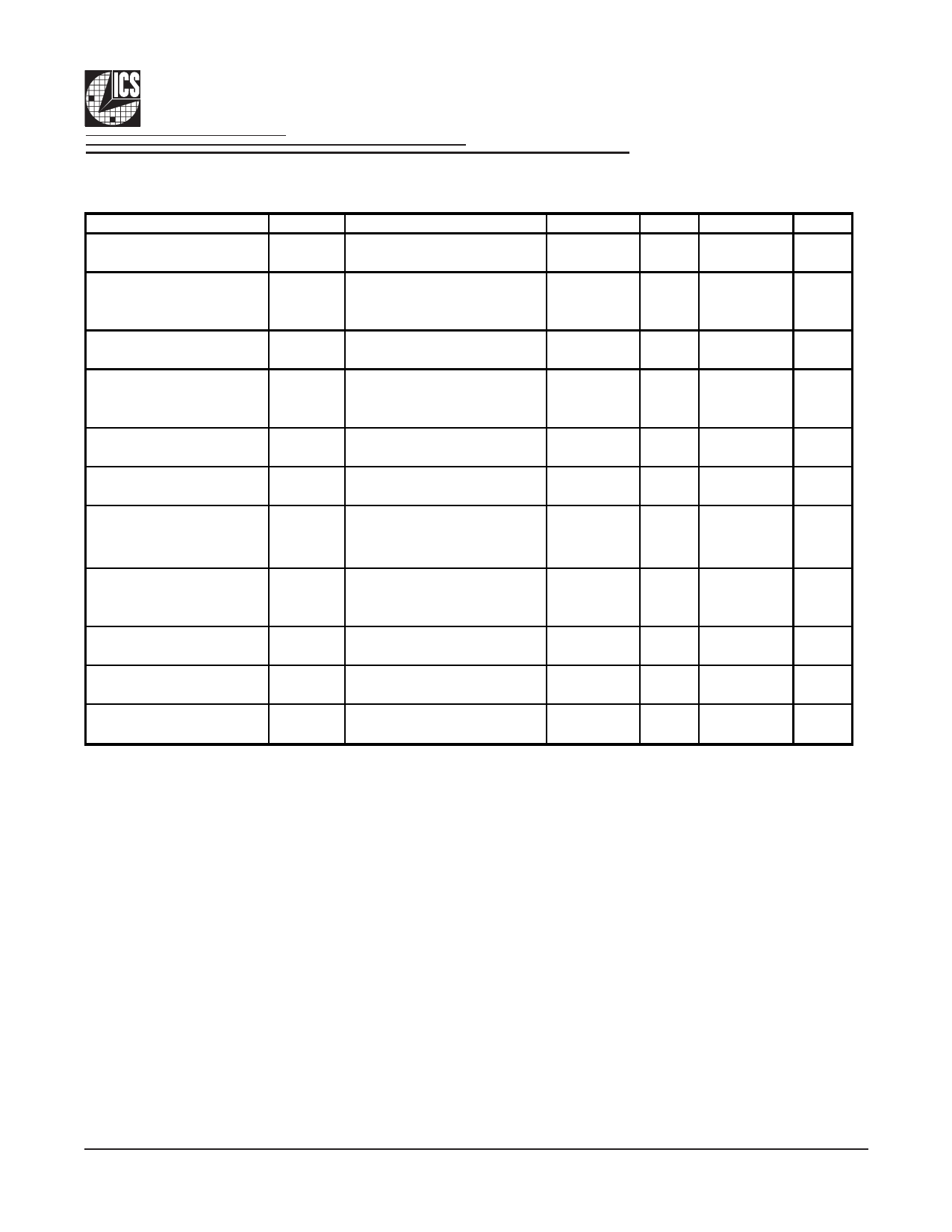
DC Characteristics - Outputs
TA = 0°C to +70°C; Supply Voltage AVDD2.5, VDD2.5 = 2.5 V +/- 0.125V (unless otherwise stated)
PARAMETER
SYMBOL
CONDITIONS
MIN
TYP
MAX
Power up latency
tPU
Power within spec to
outputs within spec
3
SMBus or Mode Select
State transition latency1
tCO
transition to outputs valid
3
and within spec
Differential output
crossing voltage
VOX
Measured as shown in Fig.
3
0.9
1.1
Output Voltage Swing
Measured as shown in Fig.
(peak-to-peak singled
ended)
VCOS
Absolute output low voltage VOLABS
Reference Voltage for
swing control current
VISET
3. Excludes over and
undershoot.
Measured at ODCLK_T/C
pins
VDD = 2.3V, VOUT = 1V
300
0.85
0.98
350
1.02
Ratio of output low
current to reference
current at typical VDD2.5
IOL/IREF
IREF is equal to VISET/RRC.
Tolerance of RRC <=+/-1%.
6.8
7
7.2
Minimum current at
VOLABS
IOLABS
Measured at ODCLK_T/C
pins with termination per
Figure 3.
45
-
Low-level output voltage
SMBus
VOLSMB
IOL = 4 mA
-
0.4
Low-level output current
SMBus
IOLSMB
VOL= 0.8 V
6
-
Tristate output current
IOZ Differential clock output pins
-
50
Notes:
There is no output latency or glitches if a value is written to an output register.
that is the same as its current contents.
UNITS
ms
ms
V
mV
V
V
-
mA
V
mA
µΑ
0809D—04/07/06
8
Share Link: 