ICL7665 Просмотр технического описания (PDF) - Intersil
Номер в каталоге
Компоненты Описание
Список матч
ICL7665 Datasheet PDF : 11 Pages
| |||
ICL7665S
Detailed Description
As shown in the Functional Diagram, the ICL7665S consists
of two comparators which compare input voltages on the
SET1 and SET2 terminals to an internal 1.3V bandgap
reference. The outputs from the two comparators drive open-
drain N-channel transistors for OUT1 and OUT2, and open-
drain P-channel transistors for HYST1 and HYST2 outputs.
Each section, the Under Voltage Detector and the Over
Voltage Detector, is independent of the other, although both
use the internal 1.3V reference. The offset voltages of the
two comparators will normally be unequal so VSET1 will
generally not quite equal VSET2.
The input impedance of the SET1 and SET2 pins are
extremely high, and for most practical applications can be
ignored. The four outputs are open-drain MOS transistors,
and when ON behave as low resistance switches to their
respective supply rails. This minimizes errors in setting up
the hysteresis, and maximizes the output flexibility. The
operating currents of the bandgap reference and the
comparators are around 100nA each.
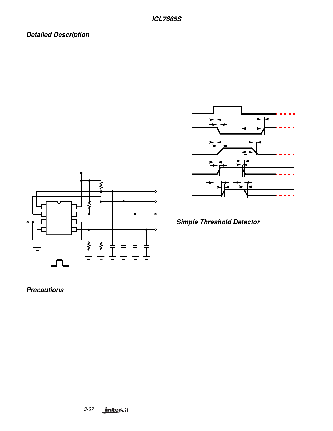
V+
1 OUT1 V+ 8
2 HYST1OUT2 7
INPUT
3 SET1 SET2 6
4 GND HYST2 5
4.7kΩ
4.7
kΩ
OUT1
HYST1
OUT2
HYST2
20 20 12 12 12 12
kΩ kΩ pF pF pF pF
1.6V
1.0V
FIGURE 7. TEST CIRCUITS
Precautions
Junction isolated CMOS devices like the ICL7665S have an
inherent SCR or 4-layer PNPN structure distributed
throughout the die. Under certain circumstances, this can be
triggered into a potentially destructive high current mode.
This latchup can be triggered by forward-biasing an input or
output with respect to the power supply, or by applying
excessive supply voltages. In very low current analog
circuits, such as the ICL7665S, this SCR can also be
triggered by applying the input power supply extremely
rapidly (“instantaneously”), e.g., through a low impedance
battery and an ON/OFF switch with short lead lengths. The
rate-of-rise of the supply voltage can exceed 100V/µs in
such a circuit. A low impedance capacitor (e.g., 0.05µF disc
ceramic) between the V+ and GND pins of the ICL7665S
can be used to reduce the rate-of-rise of the supply voltage
in battery applications. In line operated systems, the rate-of-
rise of the supply is limited by other considerations, and is
normally not a problem.
If the SET voltages must be applied before the supply
voltage V+, the input current should be limited to less than
0.5mA by appropriate external resistors, usually required for
voltage setting anyway. A similar precaution should be taken
with the outputs if it is likely that they will be driven by other
circuits to levels outside the supplies at any time.
INPUT
OUT1
VSET1,
VSET2
t SO1D
t O1F
t SO1D
t O1R
HYST1
OUT2
t SH1D
t H1R
t SO2D
t O2R
t SH2D
t H2R
HYST2
t H1F
t SH1D
t SO2D
t O2F
t SH2D
t H2F
FIGURE 8. SWITCHING WAVEFORMS
1.6V
1.0V
V+
(5V)
GND
V+
(5V)
GND
V+
(5V)
GND
V+
(5V)
GND
Simple Threshold Detector
Figure 9 shows the simplest connection of the ICL7665S for
threshold detection. From the graph 9B, it can be seen that
at low input voltage OUT1 is OFF, or high, while OUT2 is
ON, or low. As the input rises (e.g., at power-on) toward
VNOM (usually the eventual operating voltage), OUT2 goes
high on reaching VTR2. If the voltage rises above VNOM as
much as VTR1, OUT1 goes low. The equation giving VSET1
and VSET2 are from Figure 9A:
VSET1 =
VIN
R11
; VSET2 =
(R11 + R21) VIN
R12
(R12 + R22)
Since the voltage to trip each comparator is nominally 1.3V,
the value VIN for each trip point can be found from
VTR1 =
VSET1
(R11 + R21) = 1.3 (R11 + R21) for detector 1
R11
R11
and
VTR2 =
VSET2
(R12 + R22) = 1.3 (R12 + R22) for detector 2
R12
R12
3-67
Share Link: 