HT7737(2006) Просмотр технического описания (PDF) - Holtek Semiconductor
Номер в каталоге
Компоненты Описание
Список матч
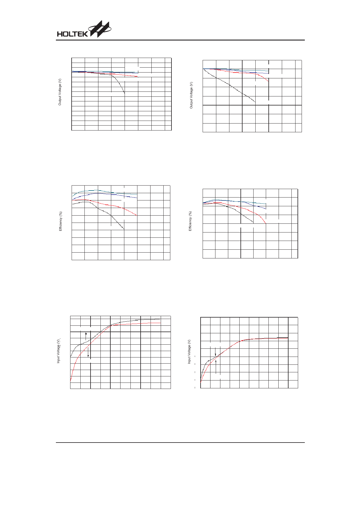
HT7737 Datasheet PDF : 15 Pages
| |||
Application Circuits
100mH
V IN
S u m id a C D - 5 4
IN 5 8 1 9
LX
H T77X X
VO UT
S e r ie s
GND
T O -9 2 /S O T -8 9
HT77XX
V OUT
22mF
100mH
V IN
S u m id a C D - 5 4
IN 5 8 1 9
LX
H T77X X
VO UT
S e r ie s
CE
NC
GND
V OUT
22mF
S O T -2 5
Note:
For the SOT-25 package, when CE is pulled low, the internal blocks of the device, such as the reference band
gap, gain block, and all feedback and control circuitry will be switched off. The boost converter¢s output, VOUT,
will be at a value one Schottky diode voltage drop below the input voltage and the LX pin remains in a high im-
pedance condition. The output capacitor and load at VOUT determine the rate at which VOUT decays.
Rev 1.10
7
March 7, 2006
Share Link: 