HPMX-2007-TR1 Просмотр технического описания (PDF) - HP => Agilent Technologies
Номер в каталоге
Компоненты Описание
Список матч
HPMX-2007-TR1 Datasheet PDF : 8 Pages
| |||
HPMX-2007 Summary Characterization Information
Standard test conditions apply unless otherwise noted.
Modulator-Only Mode
DC Current Drain
i, q Input 3 dB Bandwidth
LOmod Input Frequency Range (for Sideband Suppression > 30 dBc)
SSB Output Current (Open Collectors). See Figure 26.
SSB LOmod Suppression @ 150 MHz
DSB 3rd Order IM Products @ 150 MHz
Output Noise Floor
Typ
10
>90
40-400
2
-35
-45
-160
Units
mA
MHz
MHz
mA pk-pk diff.
dBc
dBc
dBm/Hz
Modulator + Mixer Performance (Output at 1900 MHz)
Total DC Current Drain (Mixer Cannot Be Used Without Also
Turning On the Modulator)
Mixer IF Input 3 dB Bandwidth
Differential Output Current (Open Collectors). See Figure 26.
Linear Output Power. See Figure 25.
IM3 Output Power. See Figure 19.
Output Noise Floor
LOmix Leakage to RF Output
Typ
Units
25
mA
400
MHz
12
mA pk-pk diff.
-15
dBm
-22
dBc
-153
dBm/Hz
-22
dBc
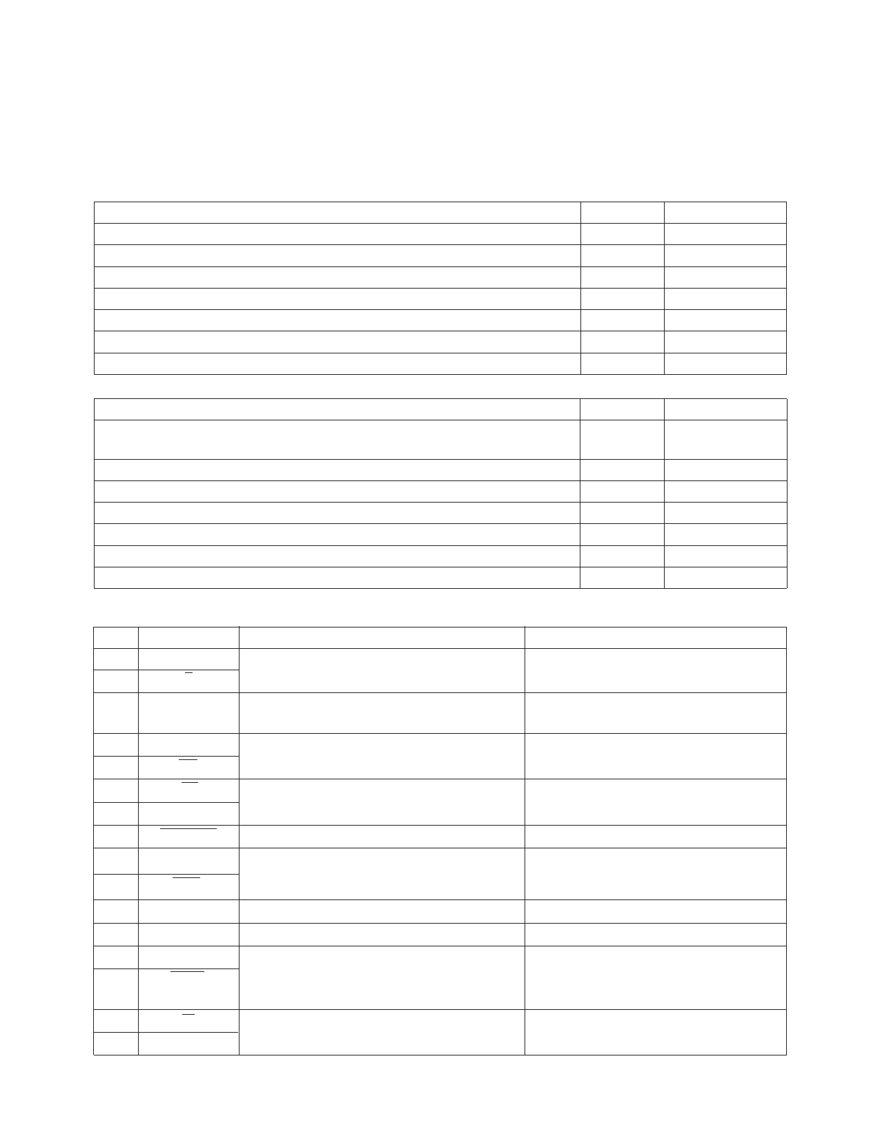
HPMX-2007 Pin Description Table
No. Mnemonic
Description
Typical Signal
1
i
Balanced modulation input
2
i
Z = 75 kΩ || 0.5 pF
600 mV pk-pk differential
average value of VCC/2
3
LOmod Modulator LO input
Z = 5 kΩ || 0.5 pF
40-400 MHz, -10 dBm from
50 Ω source
4
RF
Balanced mixer RF output open collectors 5-4000 MHz, 12 mA pk-pk differential,
5
RF
Z = current src. || 3 kΩ || 0.7 pF
with network shown in Figure 25
6
IF
Balanced mixer input
7
IF
Z = 5 kΩ || 0.5 pF
40-400 MHz, 350 mV pk-pk diff.
8
ENABLE Chip enable input
9 LOmix/mixoff Balanced mixer LO input and mixer
enable line
10
LO1
Z = 1 kΩ || 0.6 pF
11
VEE
Chip substrate connection
12
VCC
Power supply connection
13
MOD
Balanced modulator RF output
14
MOD
open collectors
Z = current src. || 35 kΩ || 0.7 pF
3 V CMOS logic compatible
-10 dBm from 50 Ω source network
shown in Figure 25
0 V (DC and AC ground)
+2.7 - 5.5 V
40-400 MHz, 2 mA pk-pk differential
with network shown in Figure 25
15
q
Balanced modulation input
16
q
Z = 75 kΩ || 0.5 pF
600 mV pk-pk differential
average value of VCC/2
Note: Impedances shown are AC equivalents at each pin, relative to ground. See Figure 26.
7-76
Share Link: 