HD74LS279FPEL Просмотр технического описания (PDF) - Renesas Electronics
Номер в каталоге
Компоненты Описание
Список матч
HD74LS279FPEL Datasheet PDF : 5 Pages
| |||
HD74LS279
Function Table
Inputs
Output
S**
R
Q
H
H
Q0
L
H
H
H
L
L
L
L
H*
Notes: 1. H; high level, L; low level
2. Q0; The level of Q before the indidicated input conditions were established.
3. *; This output level is psodo stable; that is it may not persist when S and R inputs return to their inactive
(high) level.
4. **; For latches with double S inputs; H; both S inputs high, L; one or both S inputs low.
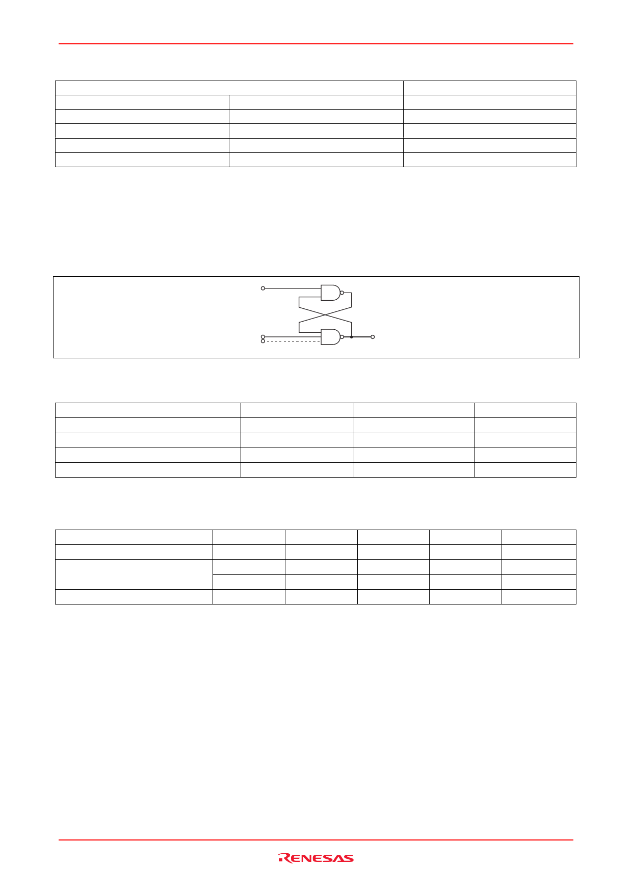
Block Diagram (1/4)
R
S1
Q
S2
Absolute Maximum Ratings
Item
Symbol
Ratings
Supply voltage
VCC
7
Input voltage
VIN
7
Power dissipation
PT
400
Storage temperature
Tstg
–65 to +150
Note: Voltage value, unless otherwise noted, are with respect to network ground terminal.
Recommended Operating Conditions
Item
Supply voltage
Output current
Operating temperature
Symbol
VCC
IOH
IOL
Topr
Min
4.75
—
—
–20
Typ
5.00
—
—
25
Max
5.25
–400
8
75
Unit
V
V
mW
°C
Unit
V
µA
mA
°C
Rev.4.00, May 10, 2006, page 2 of 4
Share Link: 