74HC4052 Просмотр технического описания (PDF) - Renesas Electronics
Номер в каталоге
Компоненты Описание
Список матч
74HC4052 Datasheet PDF : 12 Pages
| |||
HD74HC4052, HD74HC4053
Dual 4-channel Analog Multiplexers/Demultiplexers
Triple 2-channel Analog Multiplexers/Demultiplexers
REJ03D0649-0200
(Previous ADE-205-536)
Rev.2.00
Mar 30, 2006
Description
HD74HC4052: This device connects together the outputs of 4 switches in two sets, thus achieving a pair of 4 channel
multiplexers. The binary code placed on the A, and B select lines determine which switch in each 4 channel section is
“on”, connecting one of the four inputs in each section to its common output. This enables the implementation of a 4
channel differential multiplexer.
HD74HC4053: This device contains 6 switches whose outputs are connected together in pairs, thus implementing a
triple 2 channel multiplexer, or the equivalent of 3 single-pole-double throw configuration. Each of the A, B, or C
select lines independently controls one pair of switches, selecting one of the two switches to be “on”.
Features
• High Speed Operation
• Wide Operating Voltage: VCC = 2 to 6 V
• Low Quiescent Supply Current: ICC (static) = 4 µA max (Ta = 25°C)
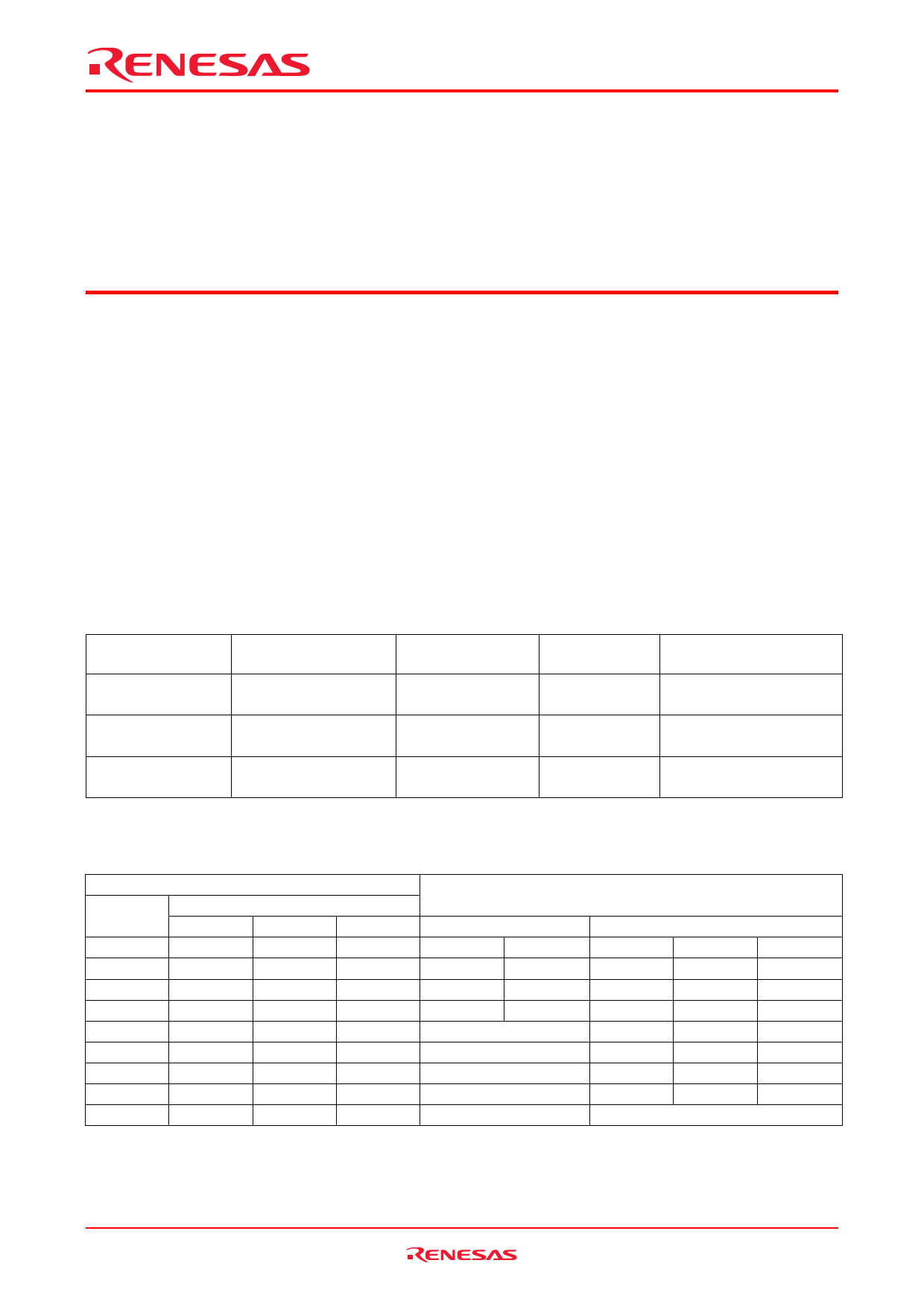
• Ordering Information
Part Name
Package Type
Package Code
(Previous Code)
Package
Abbreviation
HD74HC4052P
HD74HC4053P
DILP-16 pin
PRDP0016AE-B
P
(DP-16FV)
HD74HC4052FPEL
SOP-16 pin (JEITA)
HD74HC4053FPEL
PRSP0016DH-B
(FP-16DAV)
FP
HD74HC4052RPEL
SOP-16 pin (JEDEC)
HD74HC4053RPEL
PRSP0016DG-A
(FP-16DNV)
RP
Note: Please consult the sales office for the above package availability.
Taping Abbreviation
(Quantity)
—
EL (2,000 pcs/reel)
EL (2,500 pcs/reel)
Function Table
Control Inputs
Select
Inhibit
C*1
B
A
L
L
L
L
L
L
L
H
L
L
H
L
L
L
H
H
L
H
L
L
L
H
L
H
L
H
H
L
L
H
H
H
H
X
X
X
Note: 1. Not applicable for HD74HC4052
X = Irrelevant
HD74HC4052
Y0
X0
Y1
X1
Y2
X2
Y3
X3
—
—
—
—
—
ON Switch
HD74HC4053
Z0
Y0
X0
Z0
Y0
X1
Z0
Y1
X0
Z0
Y1
X1
Z1
Y0
X0
Z1
Y0
X1
Z1
Y1
X0
Z1
Y1
X1
—
Rev.2.00 Mar 30, 2006 page 1 of 11
Share Link: 