HD74BC640AFPEL Просмотр технического описания (PDF) - Renesas Electronics
Номер в каталоге
Компоненты Описание
Список матч
HD74BC640AFPEL Datasheet PDF : 8 Pages
| |||
HD74BC640A
Octal Bus Transceivers With 3 State Outputs
REJ03D0290–0200Z
(Previous ADE-205-026 (Z))
Rev.2.00
Jul.16.2004
Description
The HD74BC640A provides high drivability and operation equal to or better than high speed bipolar standard logic IC
by using Bi-CMOS process. The device features low power dissipation that is about 1/5 of high speed bipolar logic IC.
When the frequency is 10 MHz. The device has eight bus transceivers with three state outputs in a 20 pin package.
Each device has an active low enable input (G) and a direction control input, DiR. When DiR is high, data flows from
the A inputs to the B outputs. When DiR is high, data flows from the B inputs to the A outputs. When enable inputs
(G) is high, disables both A and B ports by placing then in a high impedance.
Features
• Input/Output are at high impedance state when power supply is off.
• Input pins can be open, when not used, owing to built in input pull up circuit.
• Input is TTL level.
• Wide operating temperature range
Ta = –40 to +85°C.
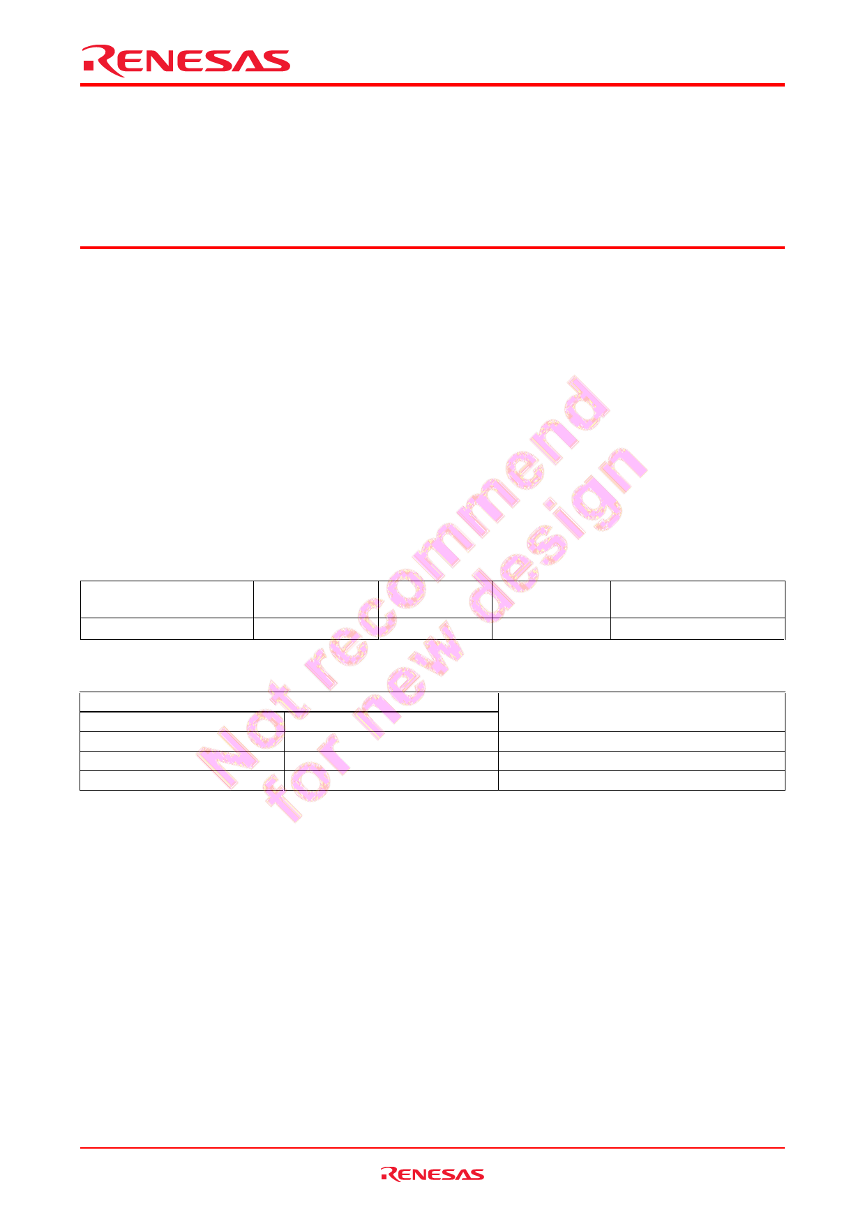
• Ordering Information
Part Name
HD74BC640AFPEL
Package Type Package Code
Package
Abbreviation
SOP-20 pin (JEITA) FP-20DAV
FP
Taping Abbreviation
(Quantity)
EL (2,000 pcs/reel)
Function Table
Control Inputs
G
DIR
L
L
L
H
H
X
H : High level
L : Low level
X : Immaterial
B data to A bus
A data to B bus
Isolation
Operation
Rev.2.00, Jul.16.2004, page 1 of 7
Share Link: 