HD6433020TE Просмотр технического описания (PDF) - Renesas Electronics
Номер в каталоге
Компоненты Описание
Список матч
HD6433020TE Datasheet PDF : 712 Pages
| |||
Item
Page
7.5.3 Pin Functions in 149
Each Mode
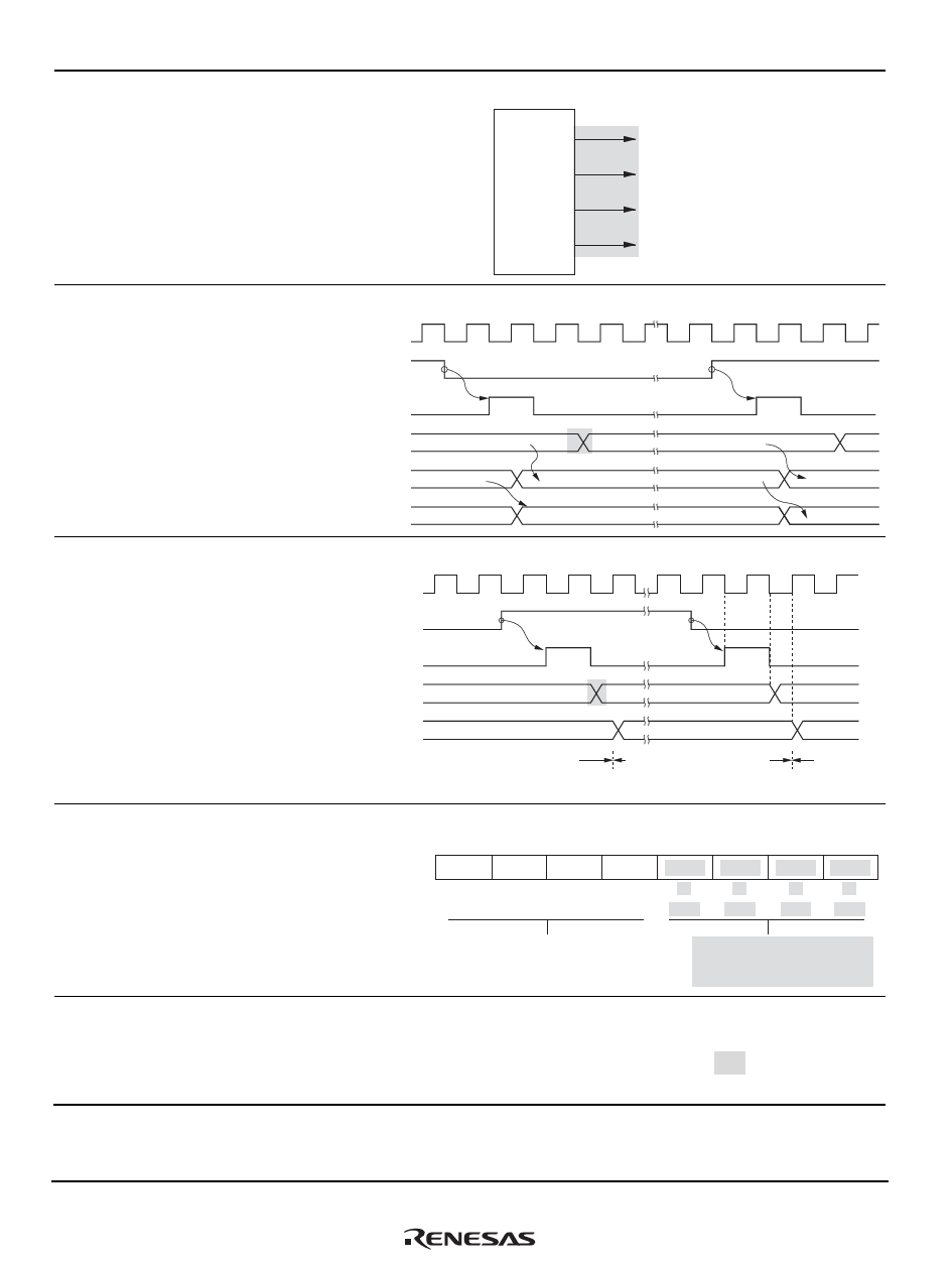
Figure 7.13 Pin
Functions in Modes 1
and 3 (Port 5)
8.4.8 Buffering
263
Figure 8.52 Input
Capture and Buffer
Transfer Timing
(Example)
8.4.9 ITU Output
266
Timing
Figure 8.55 Timing of
Disabling of ITU Output
by External Trigger
(Example)
9.2.5 Next Data
293
Register A (NDRA)
9.4.2 Note on Non- 313
Overlapping Output
Revision (See Manual for Details)
Figure amended
Port 5
A 19 (output)
A 18 (output)
A 17 (output)
A 16 (output)
Figure amended
φ
TIOC pin
Input capture
signal
TCNT
n
n+1
N
N+1
GR
M
n
n
N
BR
m
M
Figure amended
φ
M
n
TIOCA1 pin
Input capture
signal
TOER
N
H'C0
N
H'C0
ITU output
pins
ITU output
ITU output
N: Arbitrary setting (H'C1 to H'FF)
I/O port
Generic
input/output
ITU output
ITU output
I/O port
Generic
input/output
Bit table amended
Bit
Initial value
Read/Write
7
NDR7
0
R/W
6
NDR6
0
R/W
5
NDR5
0
R/W
4
NDR4
0
R/W
3
NDR3
0
R/W
2
NDR2
0
R/W
1
NDR1
0
R/W
0
NDR0
0
R/W
Next data 7 to 4
These bits store the next output
data for TPC output group 1
Next data 3 to 0
These bits store the next output
data for TPC output group 0
Description amended
This can be accomplished by having the IMFA interrupt
service routine write the next data in NDR. The next data
must be written before the next compare match B occurs.
Rev.2.00 Mar. 22, 2007 Page viii of xxiv
REJ09B0352-0200
Share Link: 