HCC4097B Просмотр технического описания (PDF) - STMicroelectronics
Номер в каталоге
Компоненты Описание
Список матч
HCC4097B Datasheet PDF : 16 Pages
| |||
HCC/HCF4067B HCC/HCF4097B
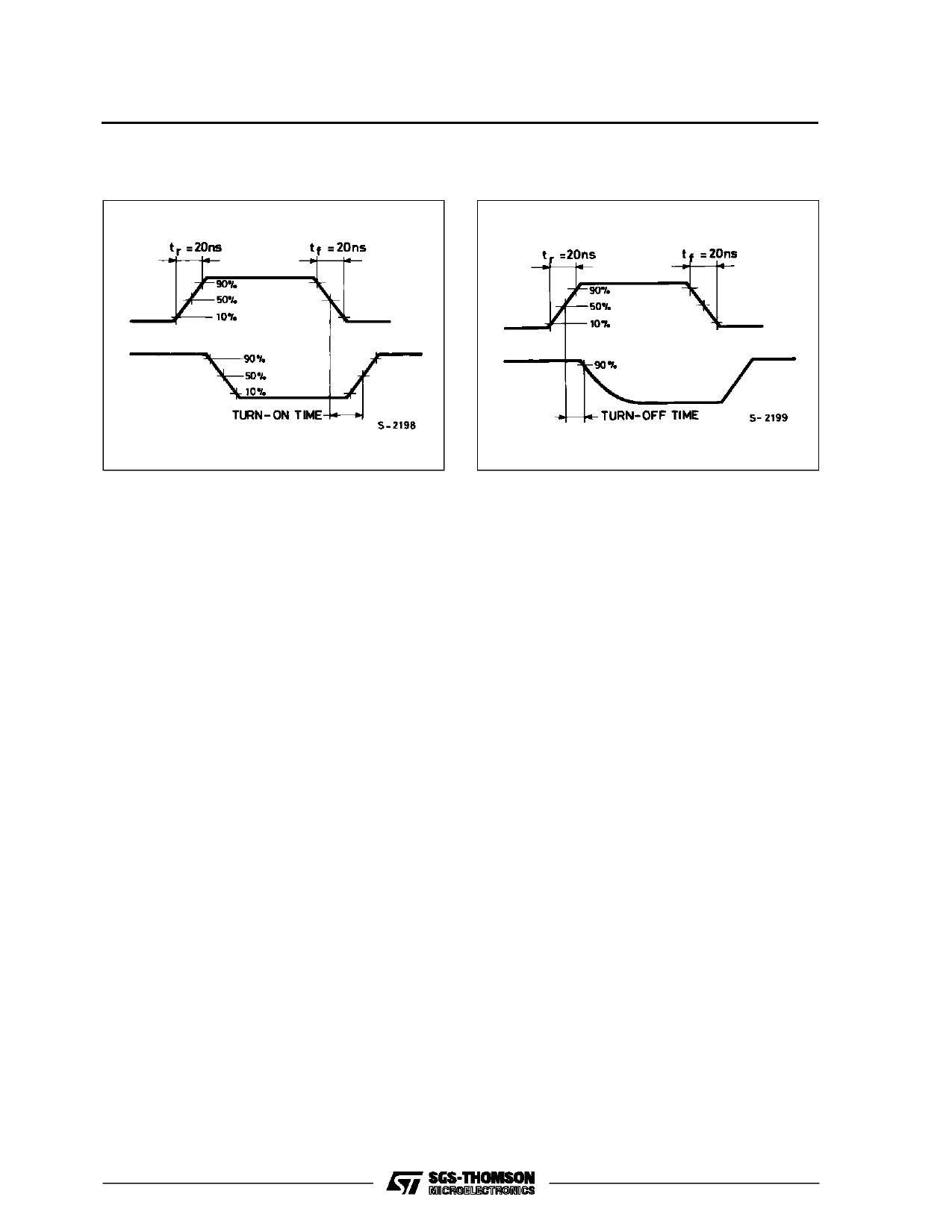
Propagation Delay Waveform Channel Being
Turned ON (RL = 10 KΩ, CL = 50 pF)
Propagation Delay Waveform Channel Being
Turned OFF (RL = 300 Ω, CL = 50 pF)
APPLICATIONS INFORMATION
In applications where separate power sources are
used to drive VDD and the signal inputs, the VDD cur-
rent capability should exceed VDD/RL (RL = effective
external load). This provision avoids permanent cur-
rent flow or clamp action on the VDD supply when
power is applied or removed from the
HCC/HCF4067B or HCC/HCF4097B.
When switching from one address to another, some
of the ON periods of the channels of the multiplexers
will overlap momentarily, which may be objection-
able in certain applications. Also when a channel is
turned ON or OFF by an address input, there is a
momentary conductive path from the channel to
VSS, which will drump some charge from any capa-
citor connected to the input or output of the channel.
The inhibit input turning on a channel will similarly
drump some charge to VSS.
The amount of charge dumped is mostly a function
of the signal level above VSS.
Typically, ay VDD - VSS = 10V, a 100 pF capacitor
connected to the input or output of the channel will
lose 3-4% of its voltage at the moment the channel
turns ON or OFF. This loss of voltage is essentially
independent of the address or inhibit signal trnasi-
tion time, if the transition time is less than 1- 2 µs.
When the inhibit signal turns a channel off, there is
no change dumping of VSS. Rather, there is a slight
rise in the channel voltage level (65 mV typ.) due to
the capacitance coupling from inhibit input to chan-
nel input or output. Address input also couple some
voltage steps onto the channel signal levels.
In certain applications, the external load-resistor
current may include both VDD and signal line com-
ponents. To avoid drawing VDD current when switch
current flows into the transmission gate inputs, the
voltage drop across the bidirectional switch must not
exceed 0.8 V (calculated from RON values shown in
ELECTRICAL CHARACTERISTICS CHART). No
VDD current will flow through RL if the switch current
flows into terminal 1 on the HCC/HCF4067B, termi-
nals 1 and 17 on the HCC/HCF4097B.
11/16
Share Link: 