GM6605 Просмотр технического описания (PDF) - Gamma Microelectronics Inc.
Номер в каталоге
Компоненты Описание
Список матч
GM6605 Datasheet PDF : 11 Pages
| |||
GM6605
5.0A LOW DROPOUT
PRECISION REGULATOR
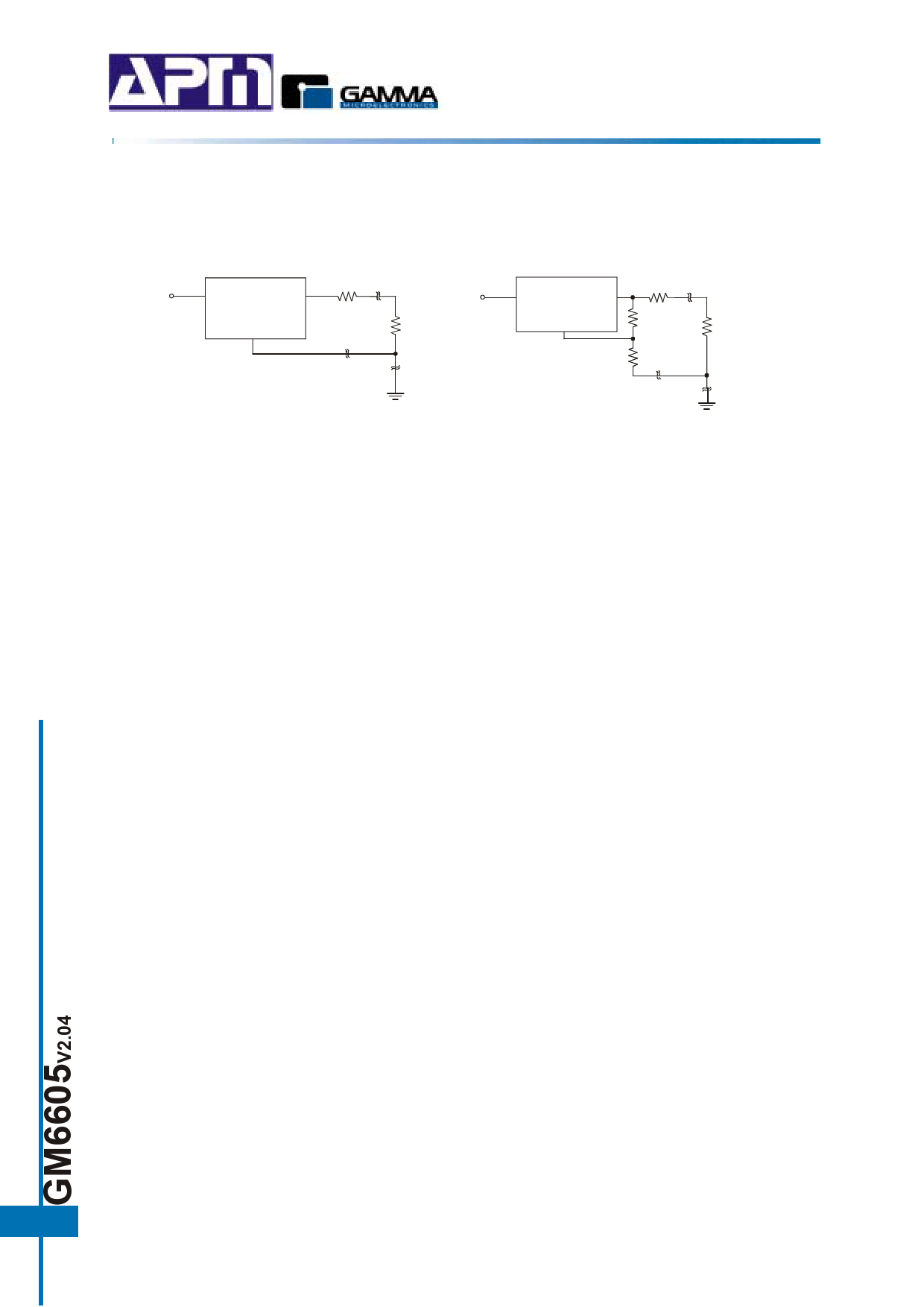
Output Voltage Sensing
GM6605 series is a three-terminal regulator, so it cannot provide true remote load sensing. Load
regulation is limited by the resistance of the conductors connecting the regulator to the load. For best
results, GM6605 should be connected as shown 1n F1gure 2.
Conductor
Parasitic
VIN
VOUT RC Resistance
GM6605-3.3
GND
RLOAD
Conductor
Parasitic
VIN
GM6605-A
VOUT RC Resistance
ADJ
R1
RLOAD
R2
(a) Fixed version
(b) Adjustable version
Figure 2. Conductor parasitic resistance effects are minimized by
this grounding scheme.
Calculating Power Dissipation and Heat Sink Requirements
GM6605 series include thermal shutdown and current limit circuitry to protect the devices. However, high
power regulators normally operate at high junction temperatures so it is important to calculate the power
dissipation and junction temperatures accurately to be sure to use an adequate heat sink. The case is
connected to VOUT on GM6605, so electrical isolation may be required for some applicat1ons. Thermal
compound should always be used with high current regulators like GM6605.
The thermal characteristics of an IC depend on four factors:
1. Maximum Ambient Temperature TA (°C)
2. Power Dissipation PD (Watts)
3. Maximum Junction Temperature TJ (°C)
4. Thermal Resistance Junction to amb1ent θJA
The relationship of these four factors is expressed by equation (1):
TJ = TA + PD x θJA
Maximum ambient temperature and power dissipation are determ1ned by the design while the maximum
junction temperature and thermal resistance depend on the manufacturer and the package type.
The maximum power dissipation for a regulator is expressed by equation (2):
PD(MAX) = (VIN(MAX) – VOUT(MIN) ) x IOUT(MIN) + VIN(MIN) x IQ
where:
VIN(MAX) is the maximum input voltage,
VOUT(MIN) is the minimum output voltage,
IOUT(MAX) is the maximum output current
IQ is the max1mum quiescent current at IOUT(MAX).
A heat sink effect1vely increases the surface area of the package to improve the flow of heat away
from the IC into the air. Each material in the heat flow path between the IC and the environment has a
thermal resistance. Like series electrical resistances, these resistance are summed to determine θJA,
the total thermal resistance between the junction and the air. This is expressed by equation (3):
θJA = θJC + θCS + θSA
where:
θJC is the thermal resistance of Junction to Case,
θCS is the thermal resistance of Case to Heat Sink,
θSA is the thermal resistance of Heat Sink to Ambient air.
The value for θJA is calculated using equation (3) and the result can be substituted in equation (1). The
value for θCS is 3.5°C/W for a given package typed based on an average d1ie size. For a high current
regulator such as GM6605, the majority of the heat is generated in the power transistor sect1on.
8
Share Link: 