MC14076BCL Просмотр технического описания (PDF) - Motorola => Freescale
Номер в каталоге
Компоненты Описание
Список матч
MC14076BCL Datasheet PDF : 6 Pages
| |||
MOTOROLA
SEMICONDUCTOR TECHNICAL DATA
MC14071B thru MC14073B,
MC14075B Ċ See Page 6-5
4-Bit D-Type Register
with Three-State Outputs
The MC14076B 4–Bit Register consists of four D–type flip–flops operating
synchronously from a common clock. OR gated output–disable inputs force
the outputs into a high–impedance state for use in bus organized systems.
OR gated data–disable inputs cause the Q outputs to be fed back to the D
inputs of the flip–flops. Thus they are inhibited from changing state while the
clocking process remains undisturbed. An asynchronous master root is
provided to clear all four flip–flops simultaneously independent of the clock
or disable inputs.
• Three–State Outputs with Gated Control Lines
• Fully Independent Clock Allows Unrestricted Operation for the Two
Modes: Parallel Load and Do Nothing
• Asynchronous Master Reset
• Four Bus Buffer Registers
• Supply Voltage Range = 3.0 Vdc to 18 Vdc
ÎÎÎÎÎÎÎÎÎÎÎÎÎÎÎÎÎÎÎÎÎ • Capable of Driving Two Low–Power TTL Loads or One Low–Power
Schottky TTL Load Over the Rated Temperature Range
ÎÎÎÎÎÎÎÎÎÎÎÎÎÎÎÎÎÎÎÎÎÎÎÎÎÎÎÎÎÎÎÎÎÎÎÎÎÎÎÎÎÎ MAXIMUM RATINGS* (Voltages Referenced to VSS)
ÎÎÎÎÎÎÎÎÎÎÎÎÎÎÎÎÎÎÎÎÎ Symbol
Parameter
Value
Unit
ÎÎÎÎÎÎÎÎÎÎÎÎÎÎÎÎÎÎÎÎÎ VDD DC Supply Voltage
– 0.5 to + 18.0
V
ÎÎÎÎÎÎÎÎÎÎÎÎÎÎÎÎÎÎÎÎÎ Vin, Vout Input or Output Voltage (DC or Transient) – 0.5 to VDD + 0.5 V
ÎÎÎÎÎÎÎÎÎÎÎÎÎÎÎÎÎÎÎÎÎ Iin, Iout Input or Output Current (DC or Transient),
± 10
mA
per Pin
ÎÎÎÎÎÎÎÎÎÎÎÎÎÎÎÎÎÎÎÎÎÎÎÎÎÎÎÎÎÎÎÎÎÎÎÎÎÎÎÎÎÎ PD Power Dissipation, per Package†
500
mW
ÎÎÎÎÎÎÎÎÎÎÎÎÎÎÎÎÎÎÎÎÎ Tstg Storage Temperature
– 65 to + 150
_C
ÎÎÎÎÎÎÎÎÎÎÎÎÎÎÎÎÎÎÎÎÎ TL
Lead Temperature (8–Second Soldering)
260
_C
ÎÎÎÎÎÎÎÎÎÎÎÎÎÎÎÎÎÎÎÎÎ * Maximum Ratings are those values beyond which damage to the device may occur.
†Temperature Derating:
Plastic “P and D/DW” Packages: – 7.0 mW/_C From 65_C To 125_C
Ceramic “L” Packages: – 12 mW/_C From 100_C To 125_C
FUNCTION TABLE
Inputs
Reset Clock
Data Disable
A
B
Data Output
D
Q
1
X
X
X
X
0
0
0
X
X
X
Qn
0
1
X
X
Qn
0
X
1
X
Qn
0
0
0
0
0
0
0
0
1
1
When either output disable A or B (or both) is (are) high the
output is disabled to the high–impedance state; however
sequential operation of the flip–flops is not affected.
X = Don’t Care.
REV 3
1/94
©MMOotoTrOolaR, IOncL. A199C5MOS LOGIC DATA
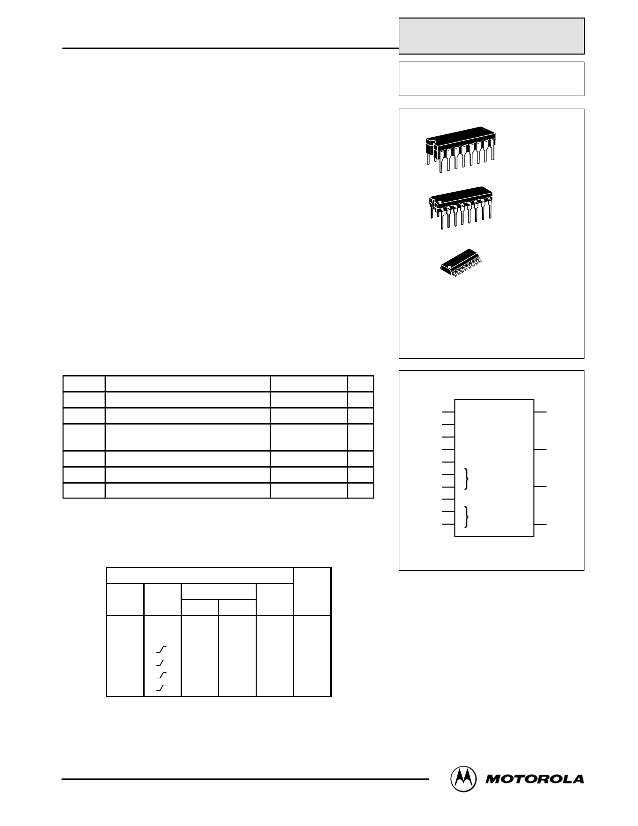
MC14076B
L SUFFIX
CERAMIC
CASE 620
P SUFFIX
PLASTIC
CASE 648
D SUFFIX
SOIC
CASE 751B
ORDERING INFORMATION
MC14XXXBCP
MC14XXXBCL
MC14XXXBD
Plastic
Ceramic
SOIC
TA = – 55° to 125°C for all packages.
BLOCK DIAGRAM
15 RESET
14 D0
13 D1
12 D2
11 D3
10 B DATA
9 A DISABLE
7 CLOCK
2 B OUTPUT
1 A DISABLE
Q0 3
Q1 4
Q2 5
Q3 6
VDD = PIN 16
VSS = PIN 8
MC14076B
1
Share Link: 