FM25V05(2012) Просмотр технического описания (PDF) - Ramtron International Corporation
Номер в каталоге
Компоненты Описание
Список матч
FM25V05 Datasheet PDF : 16 Pages
| |||
Power Up to First Access
The FM25V05 is not accessible for a period of time
(tPU) after power up. Users must comply with the
timing parameter tPU, which is the minimum time
from VDD (min) to the first /S low.
Data Transfer
All data transfers to and from the FM25V05 occur in
8-bit groups. They are synchronized to the clock
signal (C), and they transfer most significant bit
(MSB) first. Serial inputs are registered on the rising
edge of C. Outputs are driven from the falling edge of
clock C.
Command Structure
There are ten commands called op-codes that can be
issued by the bus master to the FM25V05. They are
listed in the table below. These op-codes control the
functions performed by the memory. They can be
divided into three categories. First, there are
commands that have no subsequent operations. They
perform a single function, such as to enable a write
operation. Second are commands followed by one
byte, either in or out. They operate on the Status
Register. The third group includes commands for
memory transactions followed by address and one or
more bytes of data.
Table 1. Op-code Commands
Name Description
WREN Set Write Enable Latch
WRDI Write Disable
RDSR Read Status Register
WRSR Write Status Register
READ Read Memory Data
FSTRD Fast Read Memory Data
WRITE Write Memory Data
SLEEP Enter Sleep Mode
RDID Read Device ID
SNR
Read S/N
Op-code
0000 0110b
0000 0100b
0000 0101b
0000 0001b
0000 0011b
0000 1011b
0000 0010b
1011 1001b
1001 1111b
1100 0011b
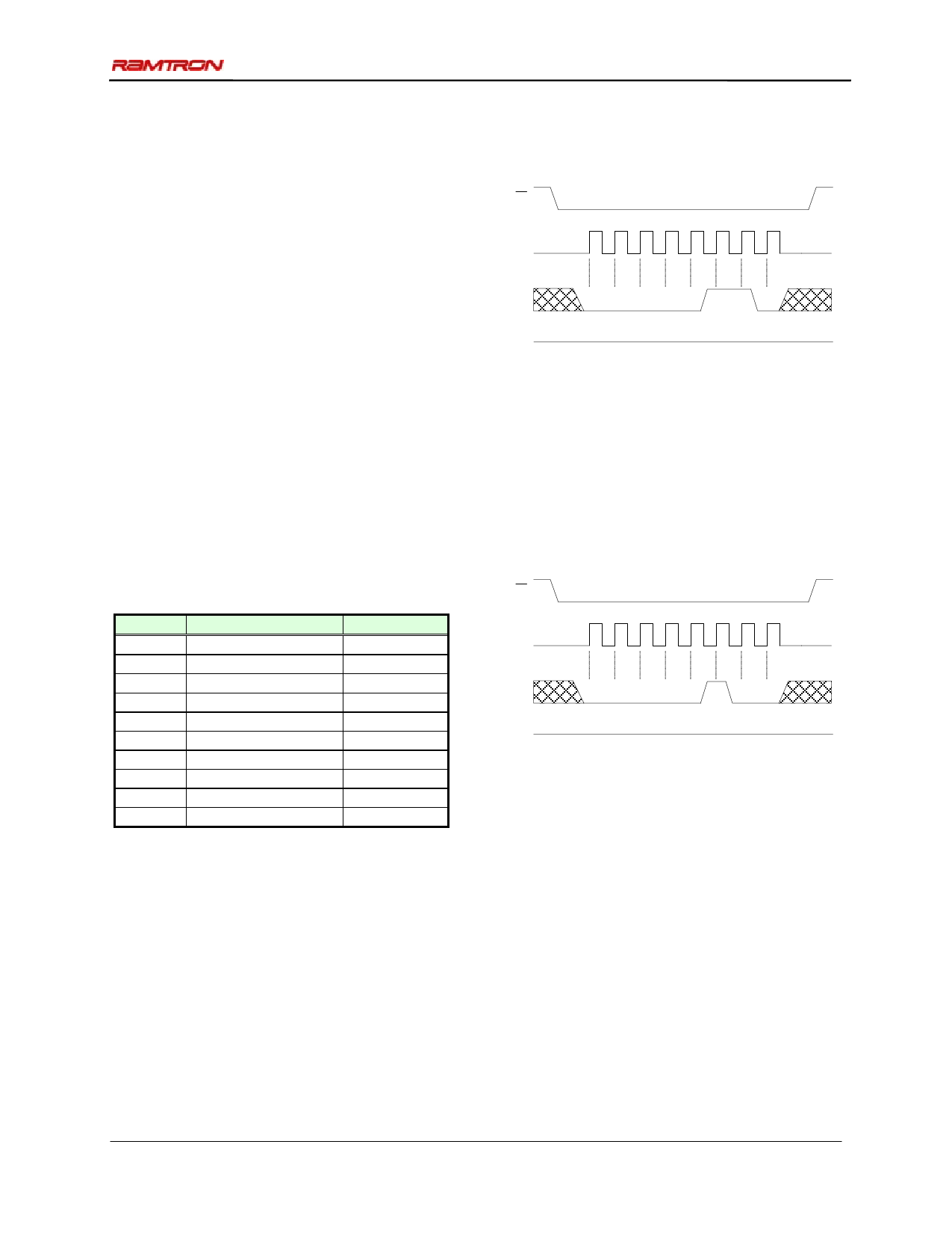
WREN – Set Write Enable Latch
The FM25V05 will power up with writes disabled.
The WREN command must be issued prior to any
write operation. Sending the WREN op-code will
allow the user to issue subsequent op-codes for write
operations. These include writing the Status Register
(WRSR) and writing the memory (WRITE).
Sending the WREN op-code causes the internal Write
Enable Latch to be set. A flag bit in the Status
Register, called WEL, indicates the state of the latch.
WEL=1 indicates that writes are permitted.
Attempting to write the WEL bit in the Status
Register has no effect on the state of this bit.
Completing any write operation will automatically
Rev. 3.0
Jan. 2012
FM25V05 - 512Kb SPI FRAM
clear the write-enable latch and prevent further
writes without another WREN command. Figure 5
below illustrates the WREN command bus
configuration.
S
01234567
C
D
00000110
Q
Hi-Z
Figure 5. WREN Bus Configuration
WRDI – Write Disable
The WRDI command disables all write activity by
clearing the Write Enable Latch. The user can verify
that writes are disabled by reading the WEL bit in
the Status Register and verifying that WEL=0.
Figure 6 illustrates the WRDI command bus
configuration.
S
01234567
C
D
00000100
Q
Hi-Z
Figure 6. WRDI Bus Configuration
RDSR – Read Status Register
The RDSR command allows the bus master to
verify the contents of the Status Register. Reading
Status provides information about the current state
of the write protection features. Following the
RDSR op-code, the FM25V05 will return one byte
with the contents of the Status Register. The Status
Register is described in detail in the section below.
Page 5 of 16
Share Link: 