FM24C64C Просмотр технического описания (PDF) - Ramtron International Corporation
Номер в каталоге
Компоненты Описание
Список матч
FM24C64C Datasheet PDF : 12 Pages
| |||
aborts the write operation and allows the read
command to be issued with the device address LSB
FM24C64C
set to a 1. The operation is now a current address
read.
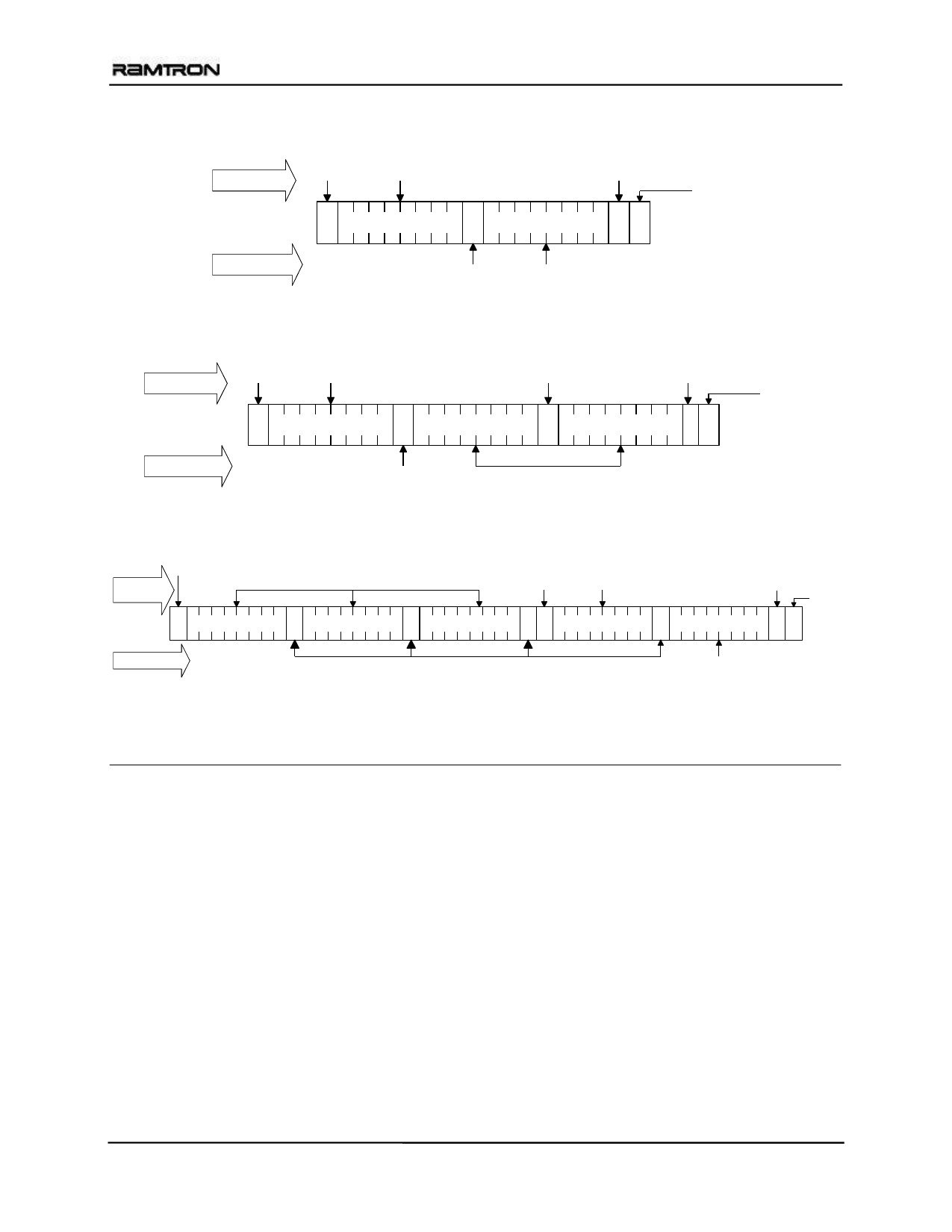
By Master
Start
Address
S
Slave Address 1 A
No
Acknowledge
Data Byte
1P
Stop
By F-RAM
Acknowledge Data
Figure 7. Current Address Read
By Master
Start
Address
S
Slave Address 1 A
Acknowledge
No
Acknowledge
Data Byte
A
Data Byte
1P
Stop
By F-RAM
Acknowledge
Data
Figure 8. Sequential Read
Start
By Master
Address
S
Slave Address 0 A X Address MSB
A
Address LSB
Start
Address
AS
Slave Address 1 A
By F-RAM
Acknowledge
No
Acknowledge
Stop
Data Byte
1P
Data
Figure 9. Selective (Random) Read
Endurance
The FM24C64C internally operates with a read and
restore mechanism. Therefore, endurance cycles are
applied for each read or write cycle. The memory
architecture is based on an array of rows and
columns. Each read or write access causes an
endurance cycle for an entire row. In the FM24C64C,
a row is 64 bits wide. Every 8-byte boundary marks
the beginning of a new row. Endurance can be
optimized by ensuring frequently accessed data is
located in different rows. Regardless, FRAM read
and write endurance is effectively unlimited at the
1MHz two-wire speed. Even at 3000 accesses per
second to the same segment, 10 years time will
elapse before 1 trillion endurance cycles occur.
Rev. 1.1
June 2011
7 of 12
Share Link: 