FM24C04 Просмотр технического описания (PDF) - Fairchild Semiconductor
Номер в каталоге
Компоненты Описание
Список матч
FM24C04 Datasheet PDF : 14 Pages
| |||
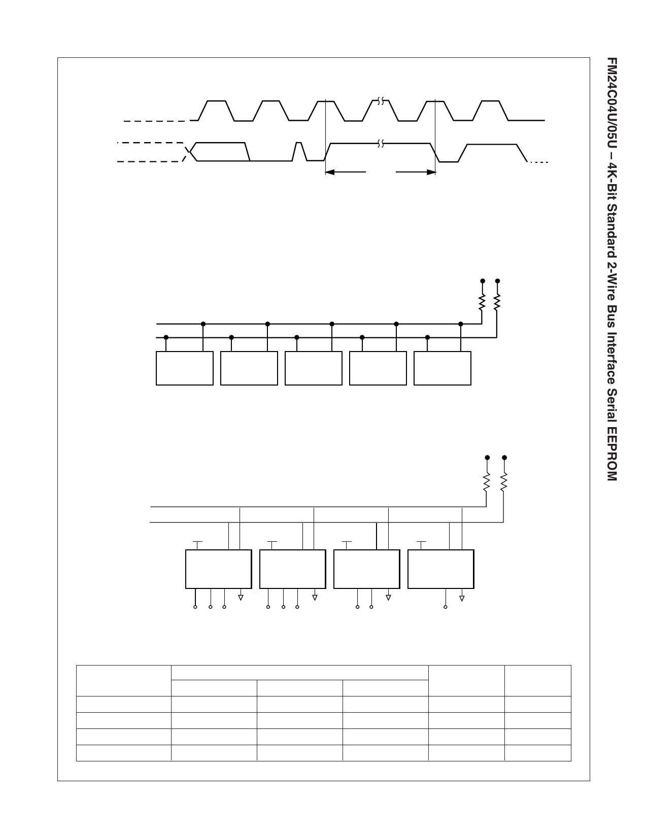
Write Cycle Timing
SCL
SDA
8th BIT
ACK
Note:
WORD n
STOP
CONDITION
tWR
START
CONDITION
The write cycle time (tWR) is the time from a valid stop condition of a write sequence to the end of the internal erase/program cycle.
Typical System Configuration
VCC
VCC
SDA
SCL
Master
Transmitter/
Receiver
Slave
Receiver
Slave
Transmitter/
Receiver
Master
Transmitter
Master
Transmitter/
Receiver
Note: Due to open drain configuration of SDA and SCL, a bus-level pull-up resistor is called for, (typical value = 4.7kΩ)
Example of 16K of Memory on 2-Wire Bus
Note:
The SDA pull-up resistor is required due to the open-drain/open collector output of IIC bus devices.
The SCL pull-up resistor is recommended because of the normal SCL line inactive 'high' state.
It is recommended that the total line capacitance be less than 400pF
VCC
VCC
SDA
SCL
VCC
VCC
VCC
VCC
24C02/03
A0 A1 A2 VSS
24C02/03
A0 A1 A2 VSS
24C04/05
A1 A2 VSS
24C08/09
A2 VSS
To To To
VSS VSS VSS
To To To
VCC VSS VSS
To To
VCC VSS
To
VCC
Device
FM24C02U/03U
FM24C04U/05U
FM24C08U/09U
FM24C16U/17U
Address Pins Present
A0
A1
A2
Yes
Yes
Yes
No
Yes
Yes
No
No
Yes
No
No
No
Memory Size
2048 Bits
4096 Bits
8192 Bits
16,384 Bits
# of Page
Blocks
1
2
4
8
6
FM24C04U/05U Rev. A.3
www.fairchildsemi.com
Share Link: 