29F040-12AI Просмотр технического описания (PDF) - Winbond
Номер в каталоге
Компоненты Описание
Список матч
29F040-12AI Datasheet PDF : 29 Pages
| |||
BRIGHT
Microelectronics
Inc.
Preliminary BM29F040
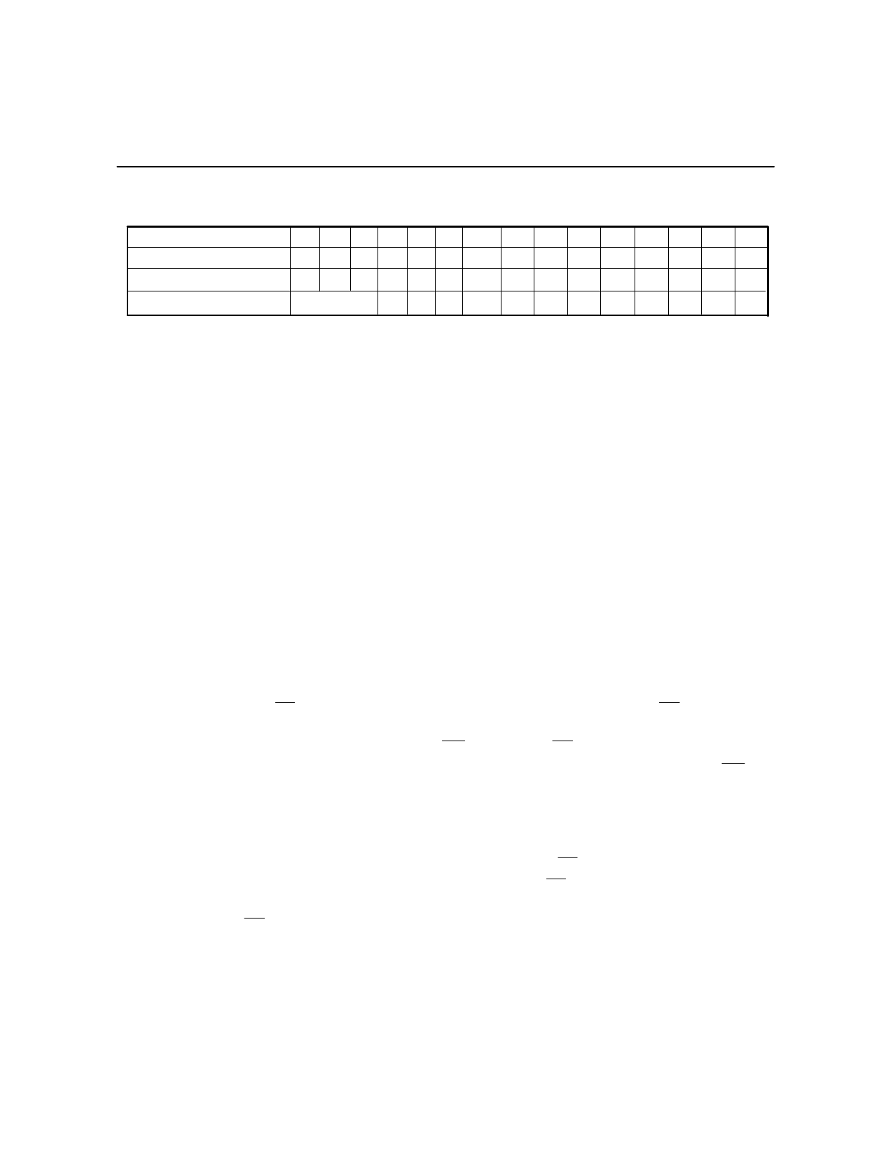
Autoselect Codes
TYPE
Manufacturer Code
BM29F040 Device code
Sector Protection (1)
A 18 A17 A 16 A 6
A1 A0
Code
(Hex)
DQ7 DQ6 DQ5 DQ4 DQ3 DQ2 DQ1 DQ0
X X X Vil Vil Vil ADH 1 0 1 0 1 1 0 1
X X X Vil Vil Vih 40H 0 1 0 0 0 0 0 0
Sector Addresses Vil Vih Vil 01H 0
0
00
00
01
Table 5
PRODUCT FAMILY PRINCIPLES OF OPERATION
Flash memory devices are electrically alterable non-volatile memory products. The BM29F040
augments this feature by not requiring an additional Vpp power supply. The 4 Megabit flash family
uses a Command register and internally generated voltages and timing algorithms to make program
and erase operations simple. The user need not worry about generating tightly controlled high
voltages on board or tying up the microcontroller to generate program and erase algorithms.
The Command register allows for 100% TTL-level control inputs, and maximum compatibility with the
Flash memory functions.
The device provides standard EPROM read, standby and output disable operations. Manufacturer
Identification and Device Identification data can be accessed through the Command register or
through the standard EPROM ″A9″ high voltage access (VID) for PROM programming equipment.
A Command register and Power Switching State Machine are built inside the device. Their purpose is
to completely automate the program and erase operation. The command register receives the
commands given by the user and internally controls the power switching state machine.
Read Mode
The BM29F040 has three control pins and they should all be logically active to obtain valid data at the
outputs. Chip-Enable ( CE ) is the device selection control. Output Enable ( OE ) is the data
input/output control. This pin when high (VIH) brings the output drivers to the tristate and allows data
into the device. Data input is then controlled by WE . When the OE pin is low (VIL) it enables the
output buffers and valid array data becomes available at the output pins. The Write Enable ( WE ) pin
has to be high during the READ mode.
Standby Mode
The BM29F040 has two standby modes: a CMOS standby mode ( CE input = Vcc +0.5V) when the
current consumed is less than 100 µA; and a TTL standby mode ( CE is held at VIH) when the current
consumed is approximately 1 mA. In the standby mode the outputs are in a high impedance state
independent of the OE input.
If the device is deselected during erasure or programming, the device will draw active current until the
erase or programming operation is complete.
-6-
Share Link: 