29F040-90AC Просмотр технического описания (PDF) - Winbond
Номер в каталоге
Компоненты Описание
Список матч
29F040-90AC Datasheet PDF : 29 Pages
| |||
BRIGHT
Microelectronics
Inc.
Preliminary BM29F040
It is also possible to determine if a sector is unprotected in the system by writing the autoselect
command and A6 is set to VIH. Performing a read operation at XXX2H and the sector address
(defined by A16, A17 and A18) will produce 00H at the Data outputs for an unprotected sector.
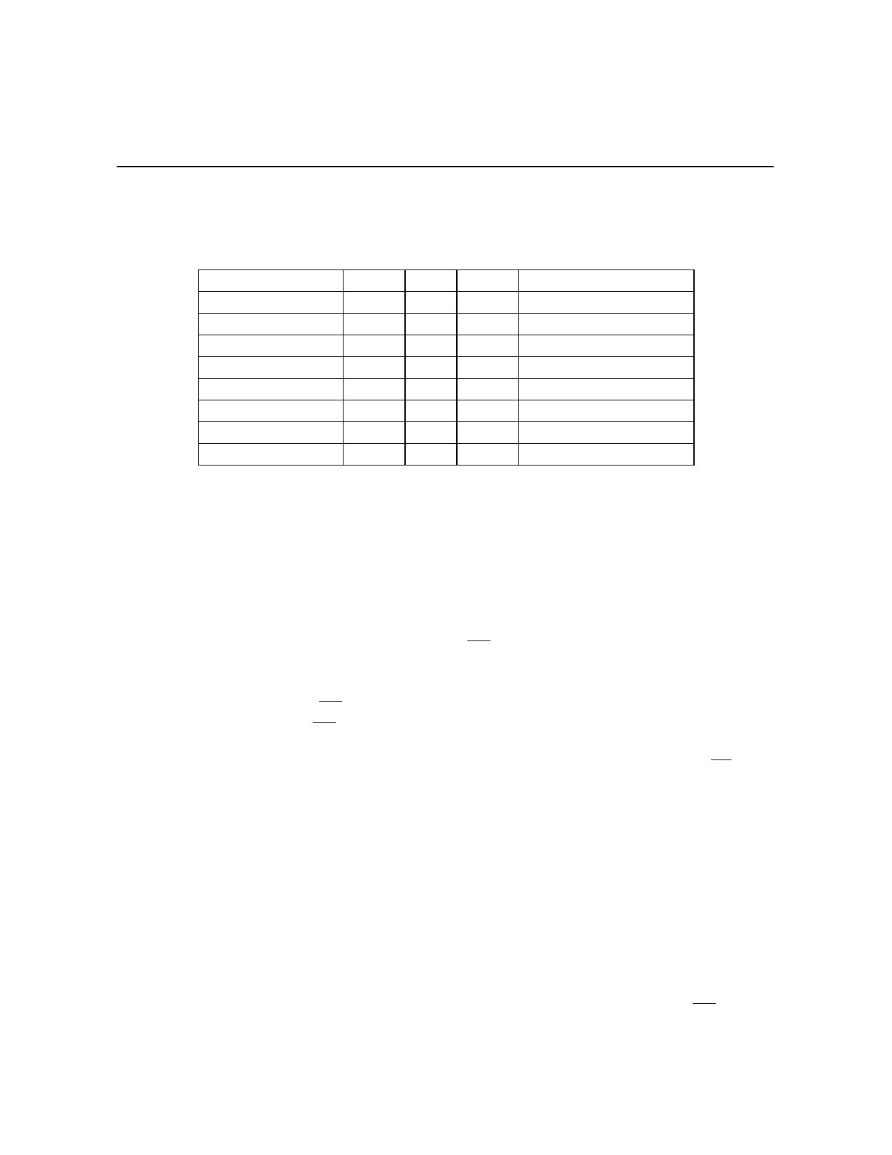
Table 7 Sector Address Table
Sector
A18
A17
A16
Address Range
SA0
0
0
0
00000H - 0FFFFH
SA1
0
0
1
10000H - 1FFFFH
SA2
0
1
0
20000H - 2FFFFH
SA3
0
1
1
30000H - 3FFFFH
SA4
1
0
0
40000H - 4FFFFH
SA5
1
0
1
50000H - 5FFFFH
SA6
1
1
0
60000H - 6FFFFH
SA7
1
1
1
70000H - 7FFFFH
Data Flags
DQ7 Data polling
The BM29F040 features Data polling to indicate to the host system that the Embedded Algorithms are
in progress or completed. During the Embedded Program Algorithm, an attempt to read the device
will produce the complement of the Data last written to DQ7. Upon completion of the Embedded
Programming Algorithm an attempt to read the device will produce the true data last written to DQ7.
Data polling is valid after the rising edge of the fourth WE pulse in the four write pulse sequence.
During the Embedded Erase Algorithm, DQ7 will be "0" until the Erase operation is completed. Upon
completion of Erase the data at DQ7 is "1". For sector erase, the Data polling is valid after the last
rising edge of the sector erase WE pulse. For Chip erase, the Data polling is valid after the last rising
edge of the sixth Chip erase WE pulse. Data polling must be performed at a sector address within
any of the sectors being erased and not a protected sector. Once the Embedded operation is close to
being completed, the BM29F040 data pins (DQ7) may change asynchronously while the OE pin is
asserted low. This means that the device is driving status information on DQ7 at one time and bytes
of valid data at other times. Depending on when the system samples the DQ7 output it may read the
status or it may read the valid data.
See Figure 12 for the Data polling timing diagram.
DQ6 Toggle Bit
The BM29F040 also features the "Toggle Bit" as a method to indicate to the host system that the
Embedded Algorithms are in progress or completed.
During an Embedded Program or Erase Algorithm cycle, successive attempts to read data from the
device will result in DQ6 toggling between "1" and "0". Once the Embedded Program or Erase
algorithm cycle is completed, DQ6 will stop toggling and valid data will be read on successive
attempts. During programming the toggle bit is valid after the rising edge of the fourth WE pulse in
A Winbond Company
- 11 -
Publication Release Date: May 1999
Revision A1
Share Link: 