ENC28J60T Просмотр технического описания (PDF) - Microchip Technology
Номер в каталоге
Компоненты Описание
Список матч
ENC28J60T Datasheet PDF : 96 Pages
| |||
ENC28J60
2.3 CLKOUT Pin
The clock out pin is provided to the system designer for
use as the host controller clock or as a clock source for
other devices in the system. The CLKOUT has an
internal prescaler which can divide the output by 1, 2,
3, 4 or 8. The CLKOUT function is enabled and the
prescaler is selected via the ECOCON register
(Register 2-1).
To create a clean clock signal, the CLKOUT pin is held
low for a period when power is first applied. After the
Power-on Reset ends, the OST will begin counting.
When the OST expires, the CLKOUT pin will begin out-
putting its default frequency of 6.25 MHz (main clock
divided by 4). At any future time that the ENC28J60 is
reset by software or the RESET pin, the CLKOUT func-
tion will not be altered (ECOCON will not change
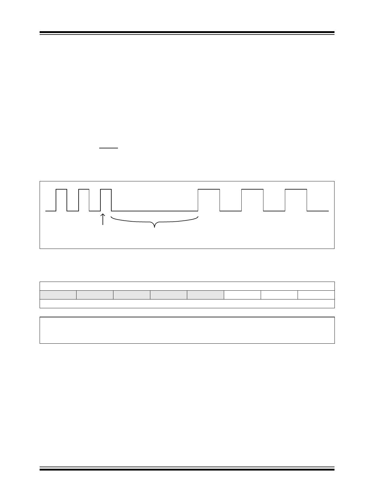
FIGURE 2-3:
CLKOUT TRANSITION
value). Additionally, Power-Down mode may be
entered and the CLKOUT function will continue to
operate. When Power-Down mode is cancelled, the
OST will be reset but the CLKOUT function will
continue. When the CLKOUT function is disabled
(ECOCON = 0), the CLKOUT pin is driven low.
The CLKOUT function is designed to ensure that mini-
mum timings are preserved when the CLKOUT pin
function is enabled, disabled or the prescaler value is
changed. No high or low pulses will be outputted which
exceed the frequency specified by the ECOCON
configuration. However, when switching frequencies, a
delay between two and eight OSC1 clock periods will
occur where no clock pulses will be produced (see
Figure 2-3). During this period, CLKOUT will be held
low.
ECOCON
Changed
80 ns to 320 ns Delay
REGISTER 2-1: ECOCON: CLOCK OUTPUT CONTROL REGISTER
U-0
U-0
U-0
U-0
U-0
R/W-1
—
—
—
—
—
COCON2
bit 7
R/W-0
COCON1
R/W-0
COCON0
bit 0
Legend:
R = Readable bit
-n = Value at POR
W = Writable bit
‘1’ = Bit is set
U = Unimplemented bit, read as ‘0’
‘0’ = Bit is cleared
x = Bit is unknown
bit 7-3
bit 2-0
Unimplemented: Read as ‘0’
COCON2:COCON0: Clock Output Configuration bits
11x = Reserved for factory test. Do not use. Glitch prevention not assured.
101 = CLKOUT outputs main clock divided by 8 (3.125 MHz)
100 = CLKOUT outputs main clock divided by 4 (6.25 MHz)
011 = CLKOUT outputs main clock divided by 3 (8.333333 MHz)
010 = CLKOUT outputs main clock divided by 2 (12.5 MHz)
001 = CLKOUT outputs main clock divided by 1 (25 MHz)
000 = CLKOUT is disabled. The pin is driven low.
DS39662B-page 6
Preliminary
© 2006 Microchip Technology Inc.
Share Link: 