EL2070 Просмотр технического описания (PDF) - Intersil
Номер в каталоге
Компоненты Описание
Список матч
EL2070 Datasheet PDF : 11 Pages
| |||
EL2070
Absolute Maximum Ratings (TA = 25°C)
Supply Voltage (VS) . . . . . . . . . . . . . . . . . . . . . . . . . . . . . . . . . . .±7V
Output Current . . . . . . . . . . . . . . . . . . . . . . . . . . . . . . . . . . . . . 70mA
(Output is short-circuit protected to ground, however, maximum reliability is
obtained if IOUT does not exceed 70mA)
Common-Mode Input Voltage . . . . . . . . . . . . . . . . . . . . . . . . . . ±VS
Differential Input Voltage . . . . . . . . . . . . . . . . . . . . . . . . . . . . . . . .5V
Disable Input Voltage . . . . . . . . . . . . . . . . . . . . . . . . . . . . . . +VS, -1V
Thermal Resistance. . . . . . . . . . . . . . . . . . . . . . . . .θJA = 95°C/W PDIP
. . . . . . . . . . . . . . . . . . . . . . . . . . . . . . . . . . . . . . . . θJA = 175°C/W SO-8
Applied Output Voltage (Disabled). . . . . . . . . . . . . . . . . . . . . . . .±VS
Power Dissipation . . . . . . . . . . . . . . . . . . . . . . . . . . . . . See Curves
Operating Temperature . . . . . . . . . . . . . . . . . . . . . . . . -40C to +85C
Pin Temperature (Soldering, 5 Seconds). . . . . . . . . . . . . . . . . 300°C
Junction Temperature . . . . . . . . . . . . . . . . . . . . . . . . . . . . . . . 175°C
Storage Temperature . . . . . . . . . . . . . . . . . . . . . . . .-60°C to +150°C
CAUTION: Stresses above those listed in “Absolute Maximum Ratings” may cause permanent damage to the device. This is a stress only rating and operation of the
device at these or any other conditions above those indicated in the operational sections of this specification is not implied.
IMPORTANT NOTE: All parameters having Min/Max specifications are guaranteed. Typical values are for information purposes only. Unless otherwise noted, all tests
are at the specified temperature and are pulsed tests, therefore: TJ = TC = TA
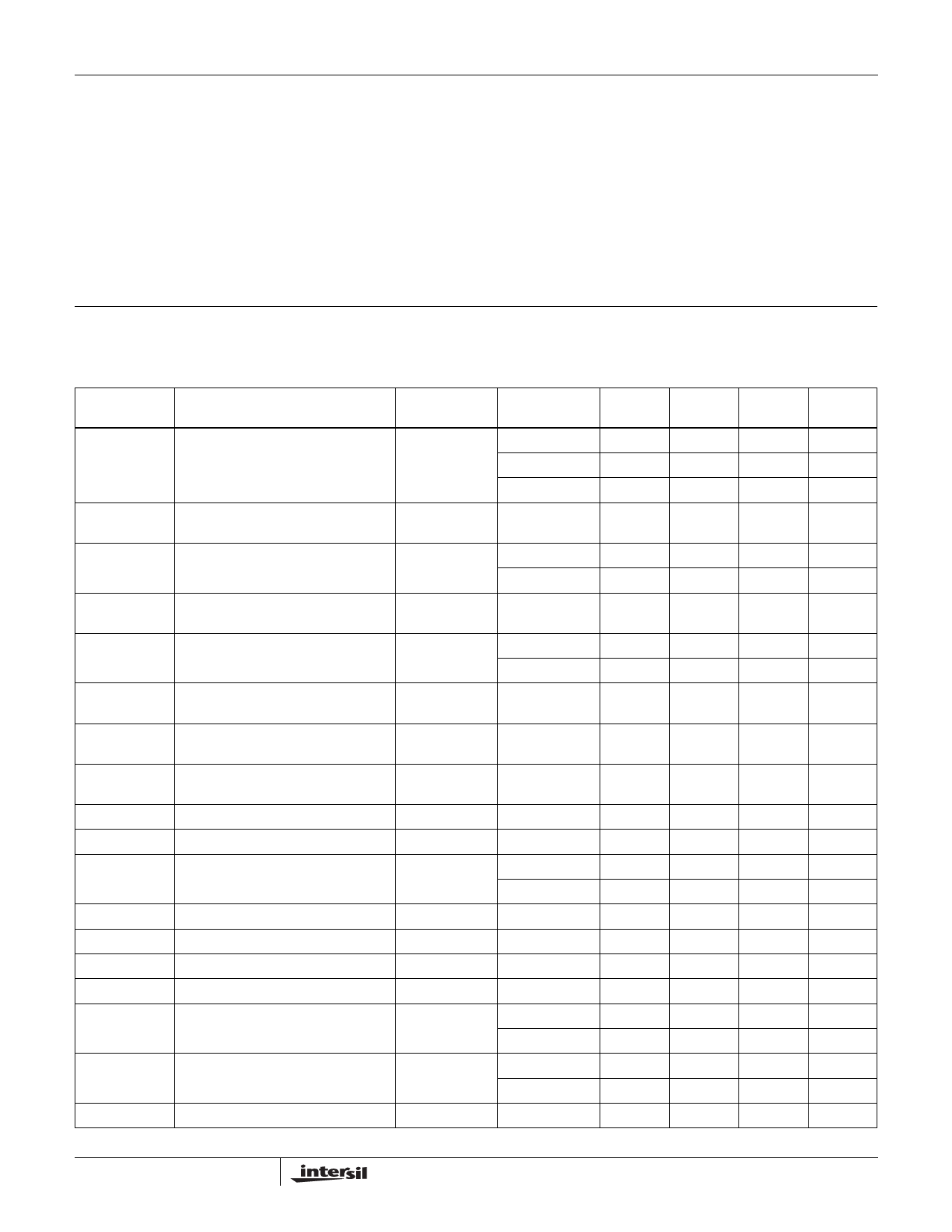
Open-Loop DC Electrical Specifications
PARAMETER
DESCRIPTION
VOS
Input Offset Voltage
d(VOS)/dT
+IIN
d(+IIN)/dT
-IIN
d(-IIN)/dT
PSRR
CMRR
IS
ISOFF
+RIN
CIN
ROUT
ROUTD
COUTD
CMIR
IOUT
VOUT
Average Offset
Voltage Drift
+Input Current
Average +Input
Current Drift
-Input Current
Average -Input
Current Drift
Power Supply
Rejection Ratio
Common-Mode
Rejection Ratio
Supply Current—Quiescent
Supply Current—Disabled
+Input Resistance
Input Capacitance
Output Impedance (DC)
Output Resistance (DC)
Output Capacitance (DC)
Common-Mode
Input Range
Output Current
Output Voltage Swing
VS = ±5V, RL = 100Ω unless otherwise specified
TEST
CONDITIONS
TEMP
MIN
TYP
25°C
2
(Note 1)
TMIN
TMAX
All
10.0
25°C, TMAX
10
TMIN
(Note 1)
All
50.0
25.0°C
10
TMIN, TMAX
(Note 1)
All
50.0
All
45.0
50.0
All
40.0
50.0
No Load
(Note 2)
Disabled
Disabled
(Note 3)
No Load
All
All
25°C, TMAX
TMIN
All
All
All
All
25°C, TMAX
TMIN
25°C, TMAX
TMIN
All
100.0
50.0
100.0
2.0
1.2
50.0
35.0
3.3
16.0
4.0
200.0
0.5
0.1
200.0
0.5
2.1
70.0
3.5
MAX
5.5
8.2
9.0
40.0
25.0
36.0
200.0
30
46
200.0
20.0
7.0
2.0
0.2
2.0
UNIT
mV
mV
mV
µV/°C
µA
µA
nA/°C
µA
µA
nA/°C
dB
dB
mA
mA
kΩ
kΩ
pF
Ω
kΩ
pF
V
V
mA
mA
V
2
Share Link: 