MB86435 Просмотр технического описания (PDF) - Fujitsu
Номер в каталоге
Компоненты Описание
Список матч
MB86435 Datasheet PDF : 36 Pages
| |||
MB86435
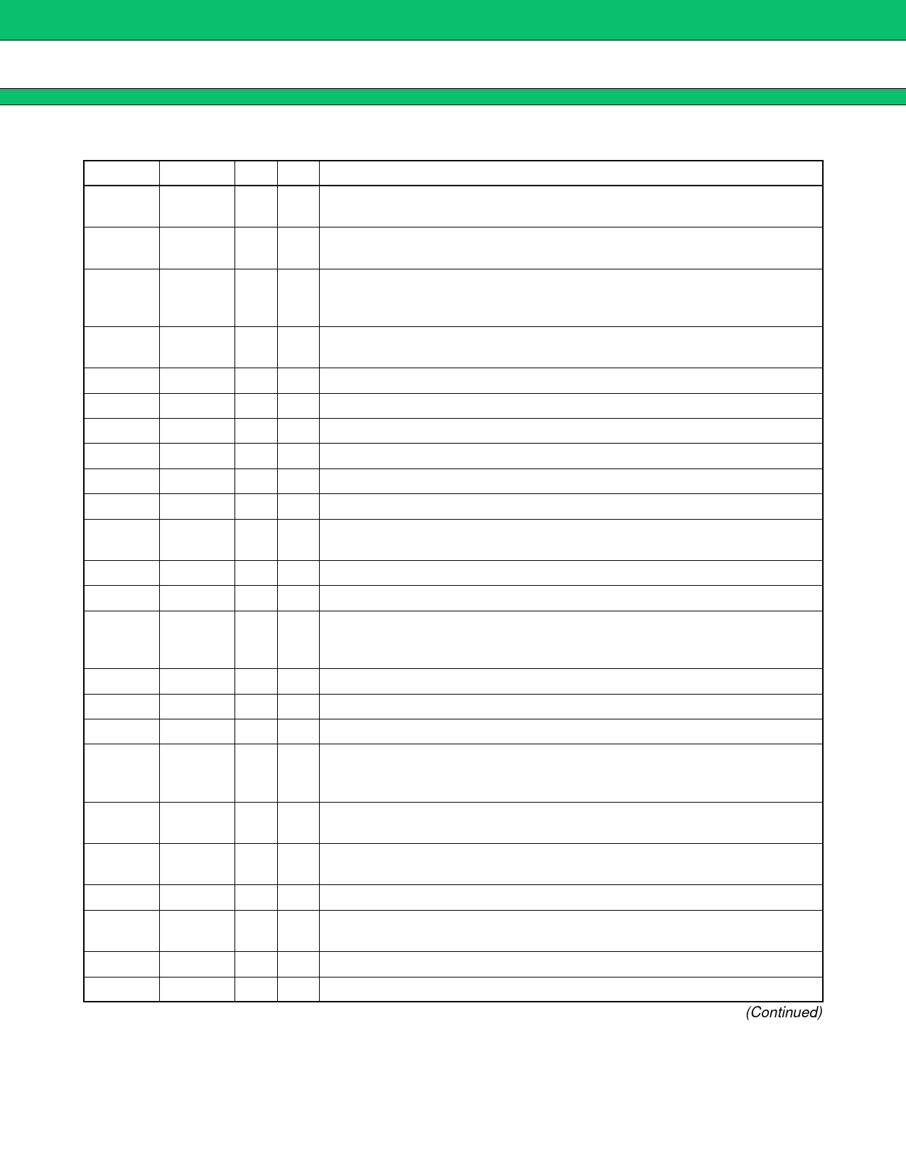
Pin No. Symbol I/O A/D
Description
21
LO2
O
D
External control latch output pin. Outputs value D2 of address 1000. CMOS
interface.
22
LO3
O
D
External control latch output pin. Outputs value D3 of address 1000. CMOS
interface.
Tone generator clock input pin. Can be used as a tone CLK signal by using
23
TCLK I D address 1110 D4D3 to subdivide the internal clock signal by factors of 1/1,
1/2, 1/4. CMOS interface.
24
TONC
I
D
Tone generator cycle control input pin. CMOS interface. Hlevel signal
outputs tone.
25
LED
O D Ring LED control output pin. CMOS interface.
26
DSCK I/O A Can be connected to EXSD or TAUD by switching bus.
27
EXSD I/O A Can be connected to DSCK or TAUD by switching bus.
28
TAUD I/O A Can be connected to EXSD or DSCK by switching bus.
29
DSDT I A Can be connected to RAUD by switching bus.
30
TONEO O A Tone signal output pin.
31
RAUD
O
A
Output pin for external speaker, or audio test signal. Can be connected to
DSDT by switching paths.
32 VDDSP1 P A Speaker amp power supply pin. To be set within range 2.7 to 3.6 V.
33
JEAR
O Earphone speaker amp output pin. Capable of 2 mW output at 32 Ω load.
Receiver speaker amp output pin. Internally connected to EAR and BTL.
34
XEAR O A Maximum output of 6.4 mW can be obtained at 32 Ω load by connecting
speaker between EAR and XEAR.
35
EAR O A Receiver speaker amp output pin. Connected to XEAR and BTL.
36
SPG1 G A Speaker amp ground pin. To be set to 0 V.
37
SPG2 G A Speaker amp ground pin. To be set to 0 V.
Speaker amp tone output pin. Internally connected to TONE and BLT.
38
XTONE O A Maximum output of 10 mW can be obtained at 25 Ω load by connecting
speaker between TONE and XTONE.
39
TONE
O
A
Speaker amp tone output pin. When speaker amp is not used for tone,
TONE should be shorted to IMTON.
40
IMTON
I
A
Speaker drive inverted (–) signal input pin. Can be used to adjust gain by
connecting resistance to TONE and IMTON.
41 VDDSP2 P A Speaker amp power supply pin. To be set within range 2.7 to 3.6 V.
42
BBI
O
A
AMP3 output pin. Should be included in HPF together with IM3, to prevent
DC offset from entering speakers.
43
IM3
I A AMP3 inverted (–) signal input pin.
44
BTO O A Receiving volume adjustment circuit output pin.
(Continued)
4
Share Link: 