DS4000 Просмотр технического описания (PDF) - Dallas Semiconductor -> Maxim Integrated
Номер в каталоге
Компоненты Описание
Список матч
DS4000 Datasheet PDF : 19 Pages
| |||
DS4000 Digitally Controlled TCXO
TEMPERATURE-COMPENSATED CRYSTAL OSCILLATOR
The DS4000 can either function as a standalone TCXO or as a digitally controlled TCXO. When used as a
standalone TCXO, the only requirements needed to function properly are power, ground, and an output. However,
the 2-wire interface must be used to tune (push and pull) the crystal.
The DS4000 is capable of supplying two different outputs, F1 and F2.
1) F1 is the base frequency of the crystal unit inside of the device. The output type is a CMOS square wave.
2) F2 is a programmable frequency output. The frequency select register can program this output to an integer
division of the base (F1) frequency. The duty cycle (DC) bit determines if the output is an n + 1 or a 2(n + 1)
division of F1.
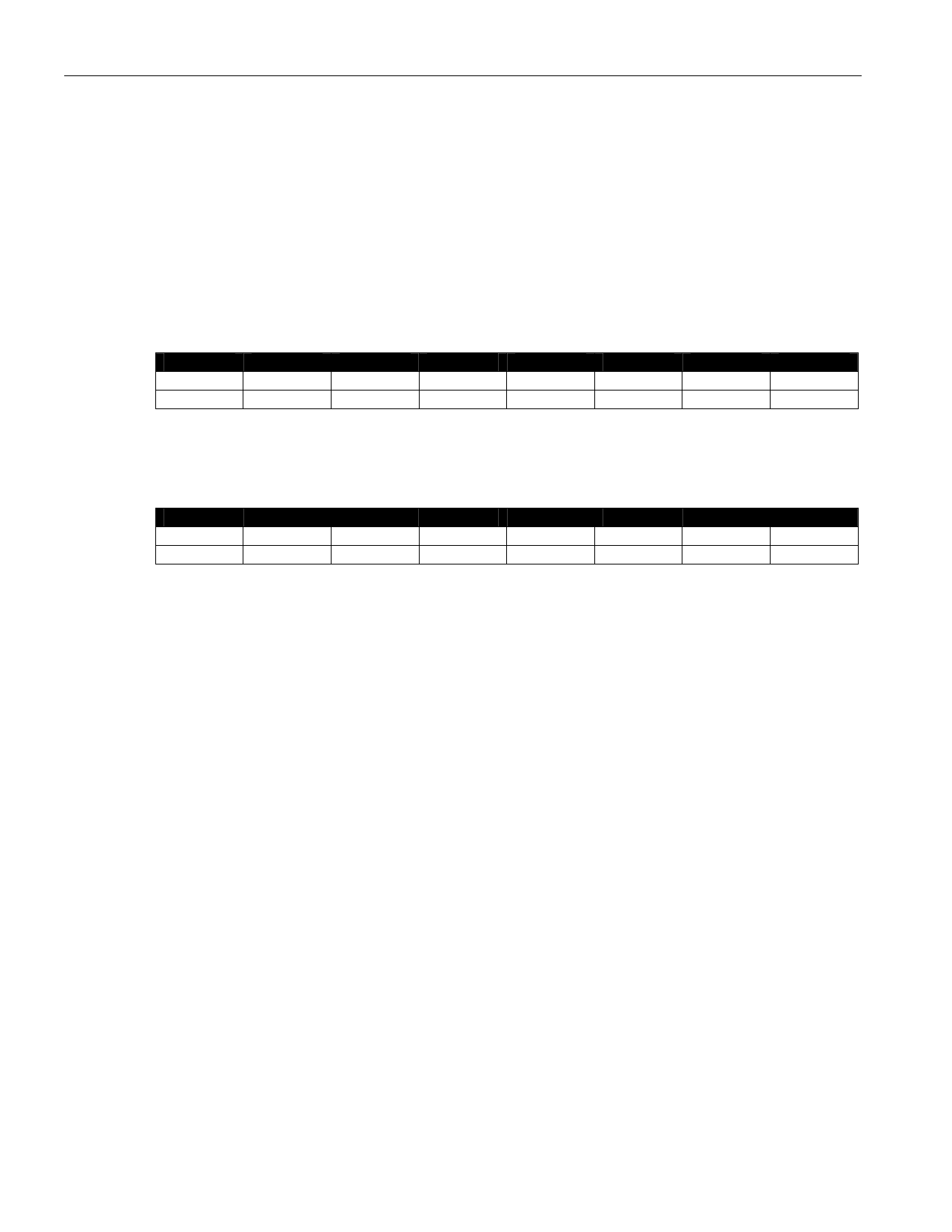
F2 FREQUENCY SELECT REGISTER (FSR) (5Dh)
Bit
7
6
5
4
3
2
1
0
Name
D7
D6
D5
D4
D3
D2
D1
D0
Default
0
0
0
0
0
0
0
0
F2 = F1 / (FSR value + 1); with DC = 0
F2 = F1 / [2 x (FSR value + 1)]; with DC = 1
TCXO CONTROL REGISTER (60h)
Bit
7
6
5
Name
X
X
X
Default
0
0
0
4
3
2
1
0
X
F2OE
F1OE
FT
DC
0
0
0
0
0
DC, Duty Cycle Bit: If 50% duty cycle is desired, then this bit must be set to logic 1. The default condition at
power-up is logic 0.
FT: This bit must be programmed by the user to 0.
F1OE, F1 Output Enable Bit: This bit allows the user to disable/enable the F1 output.
F2OE, F2 Output Enable Bit: This bit allows the user to disable/enable the F2 output.
7 of 16
Share Link: 