DS1089LU-21G(2005) Просмотр технического описания (PDF) - Maxim Integrated
Номер в каталоге
Компоненты Описание
Список матч
DS1089LU-21G Datasheet PDF : 12 Pages
| |||
3.3V Center Spread-Spectrum EconOscillator™
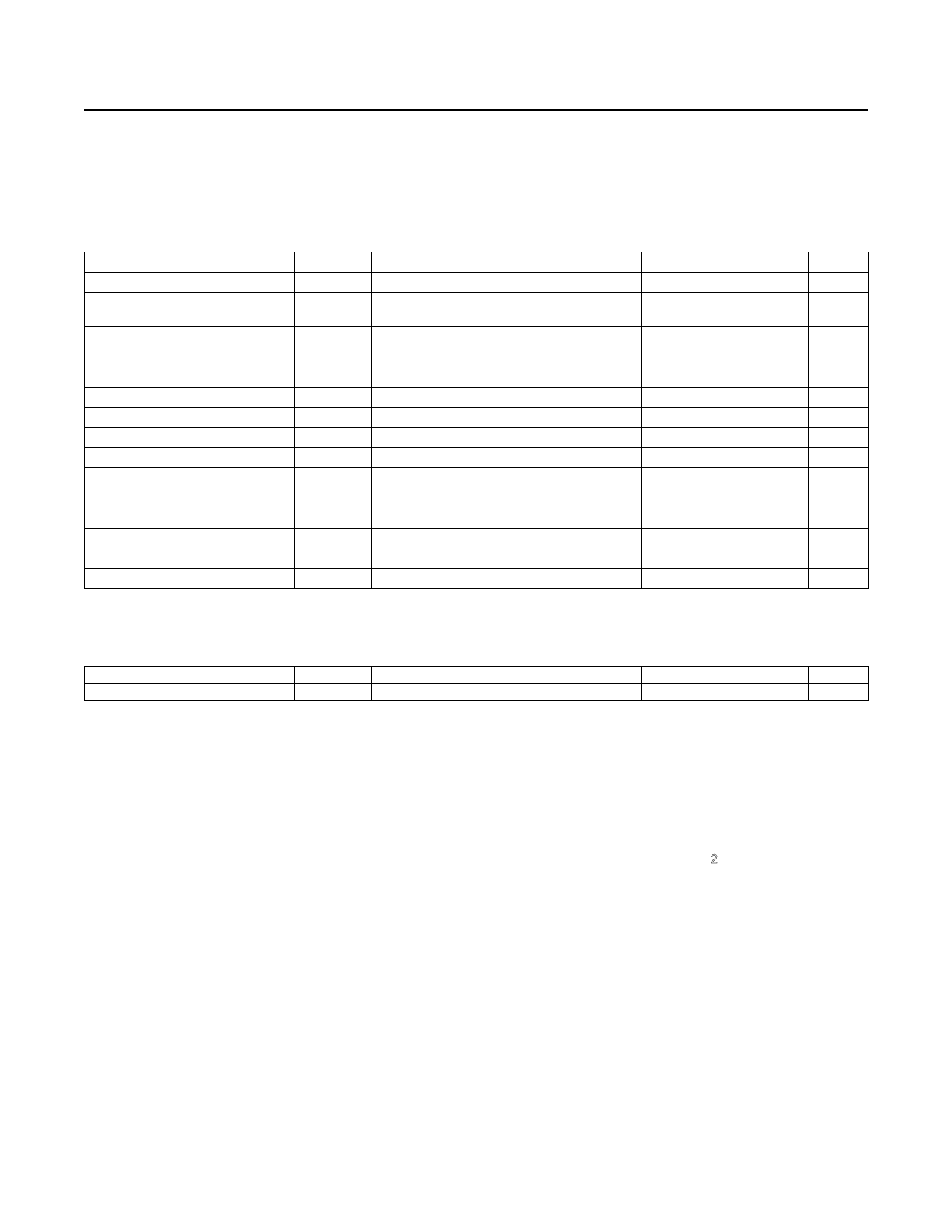
AC ELECTRICAL CHARACTERISTICS—I2C INTERFACE
(VCC = +2.7V to +3.6V, TA = -40°C to +85°C, unless otherwise noted. Timing referenced to VIL(MAX) and VIH(MIN).)
PARAMETER
SCL Clock Frequency
Bus Free Time Between Stop and
Start Conditions
SYMBOL
fSCL (Note 7)
tBUF
CONDITIONS
MIN TYP MAX
0
400
1.3
Hold Time (Repeated) Start
Condition
tHD:STA
0.6
Low Period of SCL
High Period of SCL
Data Hold Time
Data Setup Time
Start Setup Time
SDA and SCL Rise Time
SDA and SCL Fall Time
Stop Setup Time
SDA and SCL Capacitive
Loading
tLOW
tHIGH
tHD:DAT
tSU:DAT
tSU:STA
tR
tF
tSU:STO
(Note 8)
(Note 8)
CB
(Note 8)
1.3
0.6
0
0.9
100
0.6
20 + 0.1CB
300
20 + 0.1CB
300
0.6
400
EEPROM Write Time
tWR
(Note 9)
10
20
UNITS
kHz
µs
µs
µs
µs
µs
ns
µs
ns
ns
µs
pF
ms
NONVOLATILE MEMORY CHARACTERISTICS
(VCC = +2.7V to +3.6V)
PARAMETER
Writes
SYMBOL
+70°C
CONDITION
MIN
10,000
TYP
MAX UNITS
Note 1: All voltages are referenced to ground.
Note 2: This is the absolute accuracy of the master oscillator frequency at the default settings with spread disabled.
Note 3: This is the change that is observed in master oscillator frequency with changes in voltage at TA = +25°C.
Note 4: This is the change that is observed in master oscillator frequency with changes in temperature at VCC = 3.3V.
Note 5: The dither deviation of the master oscillator frequency is biderectional and results in an output frequency centered at the
undithered frequency.
Note 6: This indicates the time elapsed between power-up and the output becoming active. An on-chip delay is intentionally intro-
duced to allow the oscillator to stabilize. tSTAB is equivalent to 512 master clock cycles and will depend on the pro-
grammed master oscillator frequency.
Note 7: Timing shown is for fast-mode (400kHz) operation. This device is also backward compatible with I2C standard-mode timing.
Note 8: CB—total capacitance of one bus line in picofarads.
Note 9: EEPROM write time applies to all the EEPROM memory and SRAM shadowed EEPROM memory when WC = 0.
The EEPROM write time begins after a stop condition occurs.
4 _____________________________________________________________________
Share Link: 