DG9451(2010) Просмотр технического описания (PDF) - Vishay Semiconductors
Номер в каталоге
Компоненты Описание
Список матч
DG9451 Datasheet PDF : 13 Pages
| |||
DG9451, DG9453
Vishay Siliconix
SPECIFICATIONS FOR UNIPOLAR SUPPLIES
Parameter
Symbol
Dynamic Characteristics
Test Conditions
Unless Otherwise Specified
VIN(A,
VCC = + 12 V, VEE = 0 V
B, C and ENABLE) = 1.6 V, 0.5
Va
Temp.b
Typ.c
- 40 °C to 125 °C - 40 °C to 85 °C
Min.d Max.d Min.d Max.d Unit
Off Isolatione
Channel-to-Channel
Crosstalke
OIRR
XTALK
RL = 50 , CL = 15 pF
f = 100 kHz
Room < - 90
Room < - 90
dB
Source Off Capacitancee
CS(off)
f = 1 MHz
DG9451 Room
1
DG9453 Room
1
Drain Off Capacitancee
CD(off)
f = 1 MHz
DG9451 Room
9
DG9453 Room
3
pF
Channel On Capacitancee CD(on)
f = 1 MHz
DG9451 Room 15
DG9453 Room
8
Power Supplies
Power Supply Current
I+
Room 0.05
1
1
Full
10
10
Negative Supply Current
I-
VIN(A, B, C and ENABLE) = 0 V or 12 V
Room
Full
- 0.05
-1
- 10
-1
- 10
µA
Ground Current
IGND
Room - 0.05 - 1
-1
Full
- 10
- 10
Notes:
a. VIN = input voltage to perform proper function.
b. Room - 25 °C, Full = as determined by the operating temperature suffix.
c. Typical values are for DESIGN AID ONLY, not guaranteed nor subject to production testing.
d. The algebraic convention whereby the most negative value is a minimum and the most positive a maximum, is used in this data sheet.
e. Guaranteed by design, not subject to production test.
Stresses beyond those listed under “Absolute Maximum Ratings” may cause permanent damage to the device. These are stress ratings only, and functional operation
of the device at these or any other conditions beyond those indicated in the operational sections of the specifications is not implied. Exposure to absolute maximum
rating conditions for extended periods may affect device reliability.
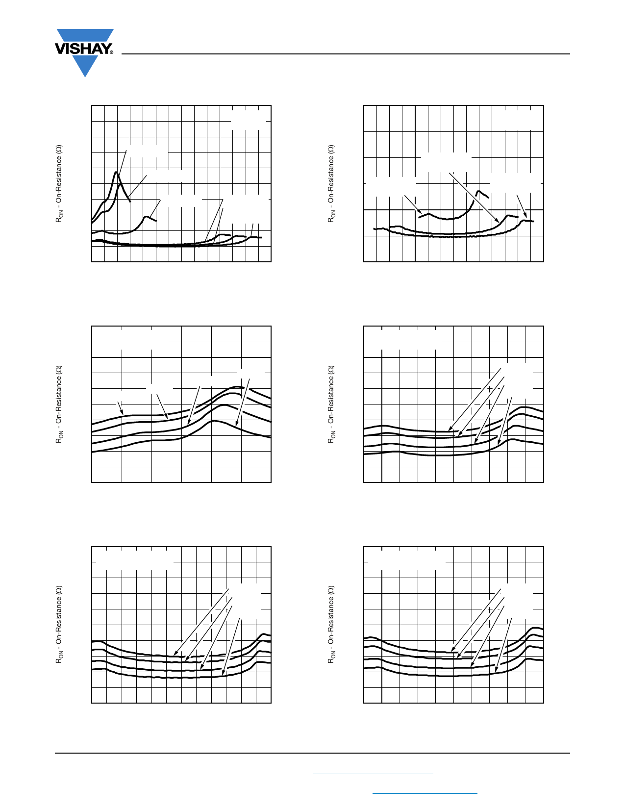
TYPICAL CHARACTERISTICS (25 °C, unless otherwise noted)
500
450
400
350
VCC = 2.7 V
T = 25 °C
IS = 1 mA
300
VCC = 3.0 V
250
200
VCC = 5.0 V
VCC = 10.8 V
VCC = 12.0 V
150
VCC = 13.2 V
100
50
0
0
2
4
6
8
10 12 14
VD - Analog Voltage (V)
On-Resistance vs. VD and Signal Supply Voltage
300
T = 25 °C
IS = 1 mA
250
200
150 VCC = + 2.7 V
VEE = - 2.7 V
VCC = + 5.0 V
VEE = - 5.0 V
100
VCC = + 6.2 V
VEE = - 6.2 V
50
0
-7 -5 -3 -1
1
3
5
7
VD - Analog Voltage (V)
On-Resistance vs. Analog Voltage and Temperature
www.vishay.com
6
Document Number: 65020
S10-2275-Rev. B, 04-Oct-10
Share Link: 