HA13158A Просмотр технического описания (PDF) - Hitachi -> Renesas Electronics
Номер в каталоге
Компоненты Описание
Список матч
HA13158A Datasheet PDF : 15 Pages
| |||
HA13158A
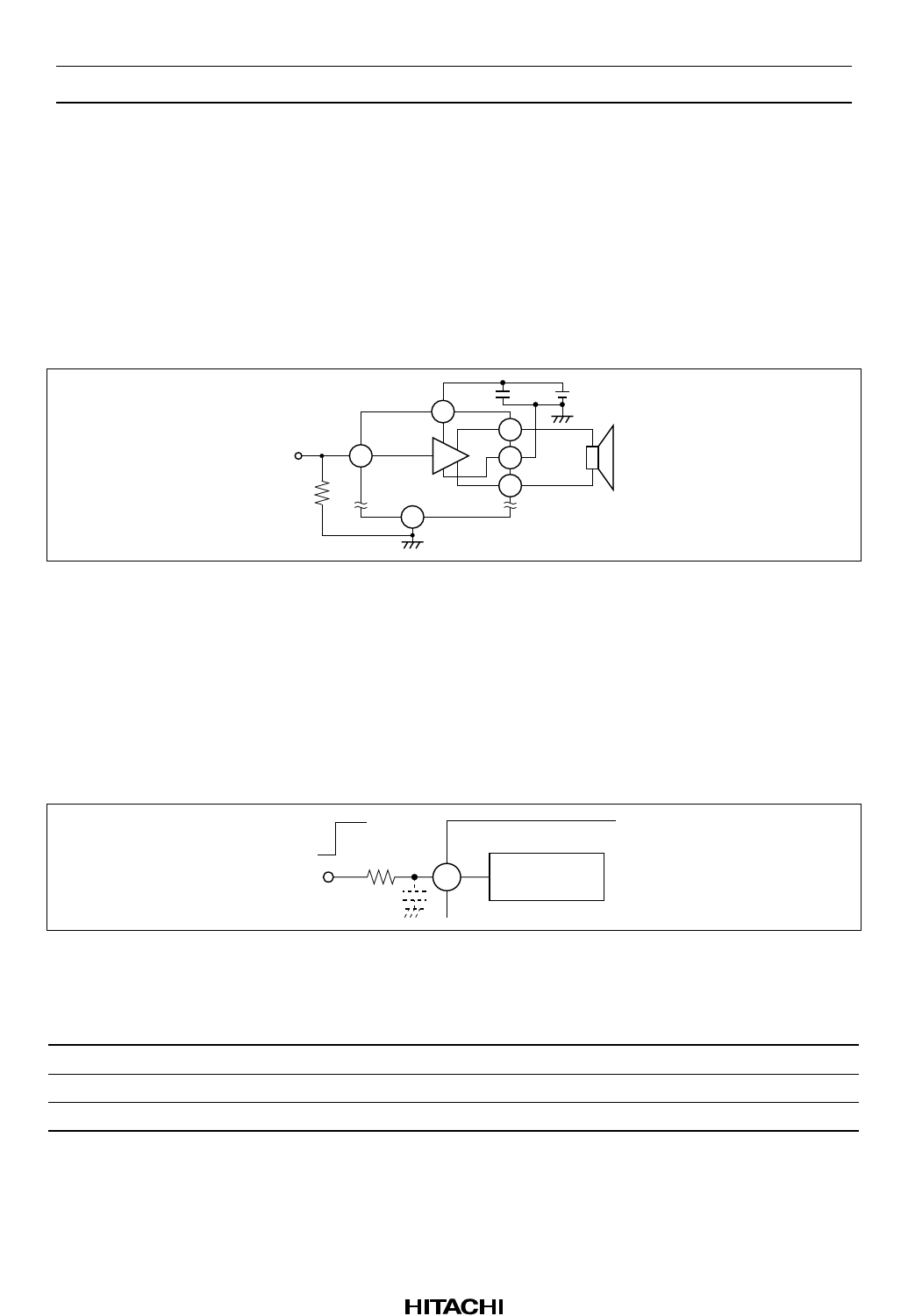
Point of Application Board Design
1. Notes on Application Board’s Pattern Design
• For increasing stability, the connected line of VCC and OUTGND is better to be made wider and lower
impedance.
• For increasing stability, it is better to place the capacitor between VCC and GND (0.1 µF) close to IC.
• It is better to place the grounding of resistor (Rg), between input line and ground, close to INGND (Pin
12) because if OUTGND is connected to the line between Rg and INGND, THD will become worse due
to current from OUTGND.
0.1 µF
VCC
6
3
1
4
Rg
5
12
Figure 1 Notes on Application Board’s Pattern Design
2. How to Reduce the Popping Noise by Muting Circuit
At normal operating circuit, Muting circuit operates at high speed under 1 µs.
In case popping noise becomes a problem, it is possible to reduce the popping noise by connecting
capacitor, which determines the switching time constant, between pin 10 and GND. (Following figure
2)
We recommend value of capacitor greater then 1 µF.
Also transitional popping noise can be reduced sharply by muting before VCC and Standby are ON/OFF.
5V
0V
7.5 kΩ
10
4.7 µF
Muting
control
Table 1
C (µF)
nothing
0.47
4.7
Figure 2 How to use Muting Circuit
Muting ON/OFF Time
ON Time
under 1 µs
2 ms
19 ms
OFF Time
under 1 µs
2 ms
19 ms
Rev.2, Jul. 1999, page 7 of 15
Share Link: 