W27E257P-10 Просмотр технического описания (PDF) - Winbond
Номер в каталоге
Компоненты Описание
Список матч
W27E257P-10 Datasheet PDF : 14 Pages
| |||
W27E257
32K × 8 ELECTRICALLY ERASABLE EPROM
GENERAL DESCRIPTION
The W27E257 is a high-speed, low-power Electrically Erasable and Programmable Read Only
Memory organized as 32768 × 8 bits that operates on a single 5 volt power supply. The W27E257
provides an electrical chip erase function. This part was the same EPROM Writer's utilities as the
W27E256.
FEATURES
• High speed access time:
100/120/150 nS (max.)
• Read operating current: 15 mA (typ.)
• Erase/Programming operating current
1 mA (typ.)
• Standby current: 5 µA (typ.)
• Single 5V power supply
• +14V erase/+12V programming voltage
• Fully static operation
• All inputs and outputs directly TTL/CMOS
compatible
• Three-state outputs
• Available packages: 28-pin 600 mil DIP and
32-pin PLCC
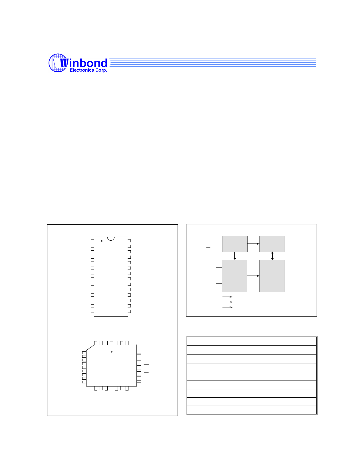
PIN CONFIGURATIONS
BLOCK DIAGRAM
VPP
A12
A7
A6
A5
A4
A3
A2
A1
A0
Q0
Q1
Q2
GND
1
28
2
27
3
26
4
25
5
24
6 28-pin 23
7 DIP
22
8
21
9
20
10
19
11
18
12
17
13
16
14
15
VCC
A14
A13
A8
A9
A11
OE
A10
CE
Q7
Q6
Q5
Q4
Q3
AV VAA
A1 PN C1 1
7 2 PC C4 3
432133 3
A6
5
2 1 0 29
A8
A5
6
A4
7
A3
8
A2
9
A1
10
A0
11
32-pin
PLCC
28
A9
27
A11
26
NC
25
OE
24
A10
23
CE
NC
Q0
12 1
13 4
11
56
11
78
1 2 22
9 0 21
Q7
Q6
Q QGN QQQ
1 2NC 3 4 5
D
CE
OE
A0
.
.
A14
VCC
GND
VPP
CONTROL
DECODER
Q0
OUTPUT
.
BUFFER
.
Q7
CORE
ARRAY
PIN DESCRIPTION
SYMBOL
A0−A14
Q0−Q7
CE
OE
VPP
VCC
GND
NC
DESCRIPTION
Address Inputs
Data Inputs/Outputs
Chip Enable
Output Enable
Program/Erase Supply Voltage
Power Supply
Ground
No Connection
Publication Release Date: January 1997
-1-
Revision A3
Share Link: 