CY7C266-45PC Просмотр технического описания (PDF) - Cypress Semiconductor
Номер в каталоге
Компоненты Описание
Список матч
CY7C266-45PC Datasheet PDF : 11 Pages
| |||
CY7C266
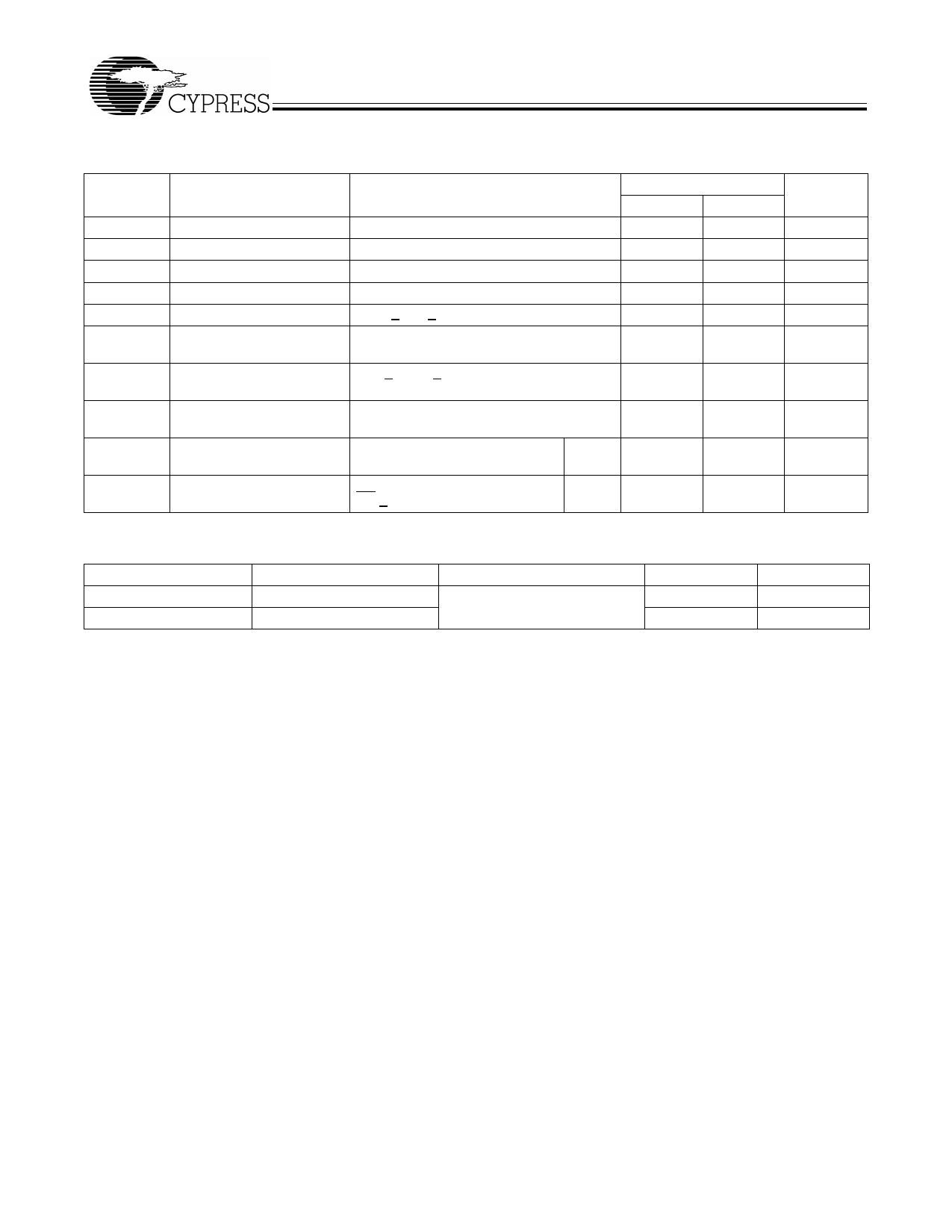
Electrical Characteristics Over the Operating Range[2] (continued)
Parameter
VOH
VOL
VIH
VIL
IIX
VCD
IOZ
Description
Output HIGH Voltage
Output LOW Voltage
Input HIGH Voltage
Input LOW Voltage
Input Current
Input Diode Clamp
Voltage
Output Leakage Current
IOS
Output Short
Circuit Current[3]
ICC
Power Supply Current
ISB
Standby Supply Current
Test Conditions
VCC = Min., IOH = –4.0 mA
VCC = Min., IOL = 16.0 mA
GND < VIN < VCC
VOL < VOUT < VOH,
Output Disabled
VCC = Max., VOUT = GND
VCC = Max., VIN = 2.0V,
IOUT = 0 mA
Chip Enable Inactive,
CE > VIH, IOUT = 0 mA
Com’l
Com’l
Capacitance[2]
Parameter
CIN
COUT
Description
Input Capacitance
Output Capacitance
Test Conditions
TA = 25°C, f = 1 MHz,
VCC = 5.0V
7C266-45
Min.
Max.
2.4
0.4
2.0
0.8
–10
+10
Note 3
–10
+10
–20
–90
100
15
Max.
10
10
Unit
V
V
V
V
mA
mA
mA
mA
mA
Unit
pF
pF
Document #: 38-04005 Rev. *B
Page 3 of 11
Share Link: 