CY7C1041BN-15ZI Просмотр технического описания (PDF) - Cypress Semiconductor
Номер в каталоге
Компоненты Описание
Список матч
CY7C1041BN-15ZI Datasheet PDF : 10 Pages
| |||
CY7C1041BN
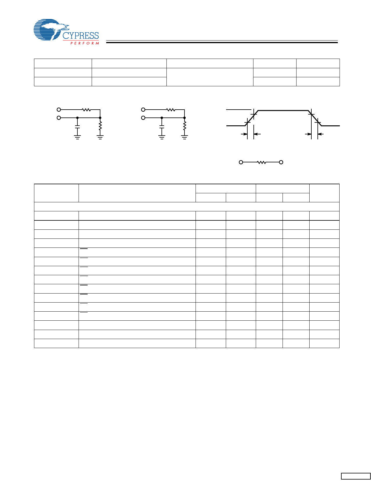
Capacitance[3]
Parameter
Description
CIN
COUT
Input Capacitance
I/O Capacitance
AC Test Loads and Waveforms
Test Conditions
TA = 25°C, f = 1 MHz,
VCC = 5.0V
Max.
Unit
8
pF
8
pF
R1 481Ω
5V
OUTPUT
30 pF
INCLUDING
JIG AND
SCOPE
(a)
R1 481Ω
5V
OUTPUT
R2
255Ω
5 pF
INCLUDING
JIG AND
SCOPE
(b)
3.0V
R2
255Ω
GND
≤ 3 ns
ALL INPUT PULSES
90%
10%
90%
10%
≤ 3 ns
Equivalent to: THÉVENIN EQUIVALENT
OUTPUT
167Ω
1.73V
Switching Characteristics[4] Over the Operating Range
-15
-20
Parameter
Description
Min.
Max.
Min.
Max.
Unit
Read Cycle
tpower
VCC(typical) to the First Access[5]
1
1
µs
tRC
Read Cycle Time
15
20
ns
tAA
Address to Data Valid
15
20
ns
tOHA
Data Hold from Address Change
3
3
ns
tACE
CE LOW to Data Valid
15
20
ns
tDOE
OE LOW to Data Valid
7
8
ns
tLZOE
tHZOE
tLZCE
tHZCE
OE LOW to Low Z
OE HIGH to High Z[6, 7]
CE LOW to Low Z[7]
CE HIGH to High Z[6, 7]
0
0
ns
7
8
ns
3
3
ns
7
8
ns
tPU
CE LOW to Power-Up
0
0
ns
tPD
CE HIGH to Power-Down
15
20
ns
tDBE
Byte Enable to Data Valid
7
8
ns
tLZBE
Byte Enable to Low Z
0
0
ns
tHZBE
Byte Disable to High Z
7
8
ns
Notes:
4. Test conditions assume signal transition time of 3 ns or less, timing reference levels of 1.5V, input pulse levels of 0 to 3.0V, and output loading of the specified
IOL/IOH and 30-pF load capacitance.
5. This part has a voltage regulator which steps down the voltage from 5V to 3.3V internally. tpower time has to be provided initially before a read/write operation is
started.
6. tHZOE, tHZCE, and tHZWE are specified with a load capacitance of 5 pF as in part (b) of AC Test Loads. Transition is measured ±500 mV from steady-state voltage.
7. At any given temperature and voltage condition, tHZCE is less than tLZCE, tHZOE is less than tLZOE, and tHZWE is less than tLZWE for any given device.
Document #: 001-06496 Rev. *A
Page 3 of 10
[+] Feedback
Share Link: 