CY62128L-70SC Просмотр технического описания (PDF) - Cypress Semiconductor
Номер в каталоге
Компоненты Описание
Список матч
CY62128L-70SC Datasheet PDF : 8 Pages
| |||
PRELIMINARY
CY62128
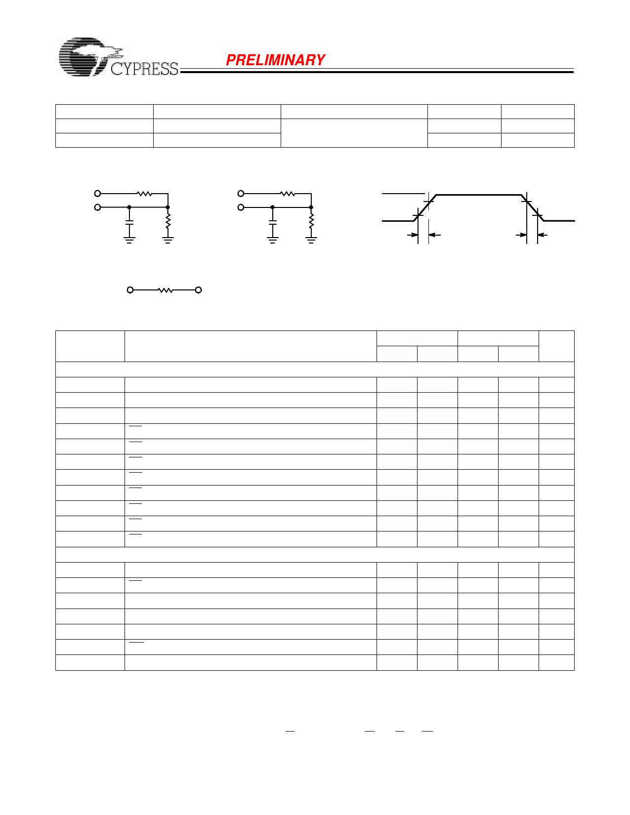
Capacitance[5]
Parameter
CIN
COUT
Description
Input Capacitance
Output Capacitance
AC Test Loads and Waveforms
Test Conditions
TA = 25°C, f = 1 MHz,
VCC = 5.0V
R1 1800 Ω
R1 1800 Ω
5V
5V
OUTPUT
100 pF
INCLUDING
JIG AND
SCOPE
(a)
OUTPUT
R2
990 Ω
5 pF
INCLUDING
JIG AND
SCOPE
(b)
R2
990 Ω
62128-3
Equivalent to: THÉVENIN EQUIVALENT
OUTPUT
639 Ω
1.77V
3.0V
GND
≤ 5ns
Max.
Unit
9
pF
9
pF
ALL INPUT PULSES
90%
10%
90%
10%
≤ 5 ns
62128-4
Switching Characteristics[3,6] Over the Operating Range
62128–55
62128–70
Parameter
Description
Min. Max. Min. Max. Unit
READ CYCLE
tRC
Read Cycle Time
tAA
Address to Data Valid
tOHA
Data Hold from Address Change
tACE
CE1 LOW to Data Valid, CE2 HIGH to Data Valid
tDOE
OE LOW to Data Valid
tLZOE
tHZOE
tLZCE
tHZCE
OE LOW to Low Z
OE HIGH to High Z[7, 8]
CE1 LOW to Low Z, CE2 HIGH to Low Z[8]
CE1 HIGH to High Z, CE2 LOW to High Z[7, 8]
tPU
CE1 LOW to Power-Up, CE2 HIGH to Power-Up
tPD
CE1 HIGH to Power-Down, CE2 LOW to Power-Down
WRITE CYCLE[9]
55
70
ns
55
70
ns
5
5
ns
55
70
ns
20
35
ns
0
0
ns
20
25
ns
5
5
ns
20
25
ns
0
0
ns
55
70
ns
tWC
Write Cycle Time
55
70
ns
tSCE
CE1 LOW to Write End, CE2 HIGH to Write End
45
60
ns
tAW
Address Set-Up to Write End
45
60
ns
tHA
Address Hold from Write End
0
0
ns
tSA
Address Set-Up to Write Start
0
0
ns
tPWE
WE Pulse Width
45
50
ns
tSD
Data Set-Up to Write End
45
55
ns
Shaded areas contain advance information
Notes:
5. Tested initially and after any design or process changes that may affect these parameters.
6. Test conditions assume signal transition time of 5ns or less, timing reference levels of 1.5V, input pulse levels of 0 to 3.0V, and output loading of the specified
IOL/IOH and 100pF load capacitance.
7. tHZOE, tHZCE, and tHZWE are specified with a load capacitance of 5 pF as in part (b) of AC Test Loads. Transition is measured ±500 mV from steady-state voltage.
8. At any given temperature and voltage condition, tHZCE is less than tLZCE, tHZOE is less than tLZOE, and tHZWE is less than tLZWE for any given device.
9. The internal write time of the memory is defined by the overlap of CE1 LOW, CE2 HIGH, and WE LOW. CE1 and WE must be LOW and CE2 HIGH to initiate a write,
and the transition of any of these signals can terminate the write. The input data set-up and hold timing should be referenced to the leading edge of the signal that terminates
the write.
3
Share Link: 