CS8126-1YDPS7 Просмотр технического описания (PDF) - ON Semiconductor
Номер в каталоге
Компоненты Описание
Список матч
CS8126-1YDPS7 Datasheet PDF : 12 Pages
| |||
CS8126
CIRCUIT DESCRIPTION
The CS8126 RESET function, has hysteresis on both the
Reset and Delay comparators, a latching Delay capacitor
discharge circuit, and operates down to 1.0 V.
The RESET circuit output is an open collector type with
ON and OFF parameters as specified. The RESET output
NPN transistor is controlled by the two circuits described
(see Block Diagram).
Low Voltage Inhibit Circuit
This circuit monitors output voltage, and when the output
voltage falls below VRT(OFF), causes the RESET output
transistor to be in the ON (saturation) state. When the output
voltage rises above VRT(ON), this circuit permits the RESET
output transistor to go into the OFF state if allowed by the
RESET Delay circuit.
RESET Delay Circuit
This circuit provides a programmable (by external
capacitor) delay on the RESET output lead. The Delay lead
provides source current to the external delay capacitor only
when the “Low Voltage Inhibit” circuit indicates that output
voltage is above VRT(ON). Otherwise, the Delay lead sinks
current to ground (used to discharge the delay capacitor).
The discharge current is latched ON when the output voltage
falls below VRT(OFF). The Delay capacitor is fully
discharged anytime the output voltage falls out of
regulation, even for a short period of time. This feature
ensures a controlled RESET pulse is generated following
detection of an error condition. The circuit allows the
RESET output transistor to go to the OFF (open) state only
when the voltage on the Delay lead is higher than VDC(H1).
The Delay time for the RESET function is calculated from
the formula:
Delay time + CDelay
VDelayThreshold
ICharge
Delay time + CDelay 3.2 105
If CDelay = 0.1 mF, Delay time (ms) = 32 ms ± 50%: i.e.
16 ms to 48 ms. The tolerance of the capacitor must be taken
into account to calculate the total variation in the delay time.
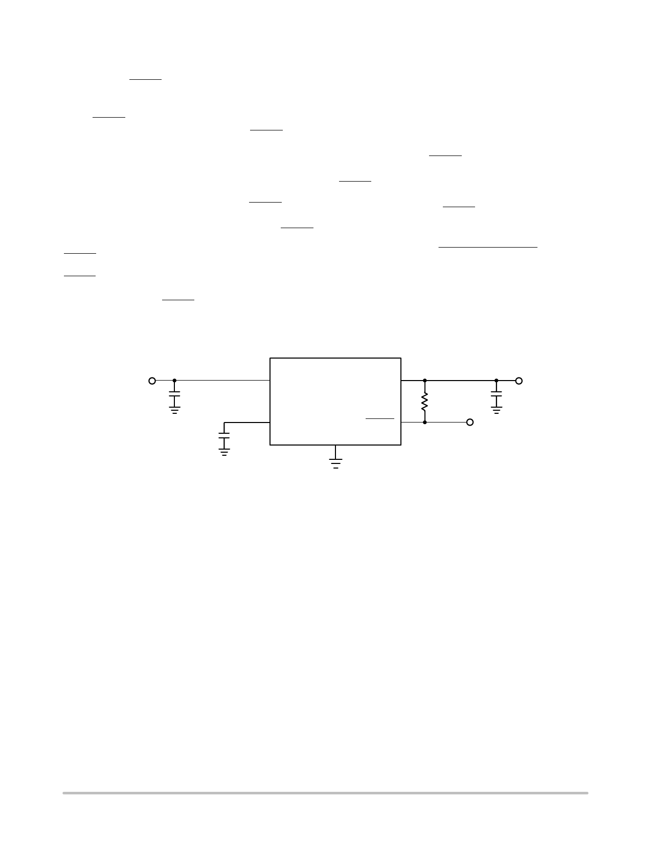
C1*
100 nF
VIN
Delay
0.1 mF
Delay
CS8126
VOUT
GND
RESET
RRST
4.7 kW
C2**
10 mF to 100 mF
* C1 is required if the regulator is far from the power source filter.
** C2 is required for stability.
Figure 13. Application Diagram
APPLICATION NOTES
Stability Considerations
The output or compensation capacitor helps determine
three main characteristics of a linear regulator: start−up
delay, load transient response and loop stability.
The capacitor value and type should be based on cost,
availability, size and temperature constraints. A tantalum or
aluminum electrolytic capacitor is best, since a film or
ceramic capacitor with almost zero ESR, can cause
instability. The aluminum electrolytic capacitor is the least
expensive solution, but, if the circuit operates at low
temperatures (−25°C to −40°C), both the value and ESR of
the capacitor will vary considerably. The capacitor
manufacturers data sheet usually provides this information.
The value for the output capacitor C2 shown in the test and
applications circuit should work for most applications,
however it is not necessarily the optimized solution.
To determine an acceptable value for C2 for a particular
application, start with a tantalum capacitor of the
recommended value and work towards a less expensive
alternative part.
http://onsemi.com
7
Share Link: 