CS8122 Просмотр технического описания (PDF) - Cherry semiconductor
Номер в каталоге
Компоненты Описание
Список матч
CS8122 Datasheet PDF : 8 Pages
| |||
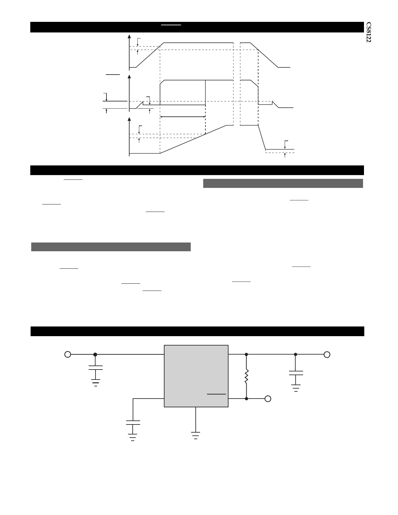
VOUT
VRT(ON)
VRT(OFF)
RESET Circuit Waveform
VRH
RESET
(3)
VRL
Delay
VDC(HI)
VDC(LO)
VDH
(1)
(2)
tDelay
(2)
(1) = No Delay Capacitor
(2) = With Delay Capacitor
(3) = Max: RESET Voltage (1.0V)
VDIS
Circuit Description
The CS8122 RESET function, has hysteresis on both the
reset and delay comparators, a latching Delay capacitor
discharge circuit, and operates down to 1V.
The RESET circuit output is an open collector type with
ON and OFF parameters as specified. The RESET output
NPN transistor is controlled by the two circuits described
(see Block Diagram).
Low Voltage Inhibit Circuit
The Low Voltage Inhibit Circuit monitors output voltage,
and when output voltage is below the specified minimum,
causes the RESET output transistor to be in the ON (satu-
ration) state. When the output voltage is above the speci-
fied level, this circuit permits the RESET output transistor
to go into the OFF state if allowed by the RESET Delay cir-
cuit.
Reset Delay Circuit
The Reset Delay Circuit provides a programmable (by
external capacitor) delay on the RESET output lead. The
Delay lead provides source current to the external delay
capacitor only when the Low Voltage Inhibit circuit indi-
cates that output voltage is above VRT(ON). Otherwise, the
Delay lead sinks current to ground (used to discharge the
delay capacitor). The discharge current is latched ON
when the output voltage is below VRT(OFF). The Delay
capacitor is fully discharged anytime the output voltage
falls out of regulation, even for a short period of time. This
feature ensures that a controlled RESET pulse is generated
following detection of an error condition. The circuit
allows the RESET output transistor to go to the OFF (open)
state only when the voltage on the Delay lead is higher
than VDC(HI).
CIN*
100nF
CDelay
0.1mF
Test Circuit
VIN
VOUT
CS8122
Delay Gnd RESET
RRST
4.7kW
COUT**
10mF
*CIN required if regulator is far from power source filter.
**COUT required for stability.
5
Share Link: 