CS5334 Просмотр технического описания (PDF) - Cirrus Logic
Номер в каталоге
Компоненты Описание
Список матч
CS5334 Datasheet PDF : 20 Pages
| |||
CS5334 CS5335
SYSTEM DESIGN
The CS5334 and CS5335 are 20-bit, 2-channel
Analog-to-Digital Converters designed for digital
audio applications. These devices use two one-
bit delta-sigma modulators which simultaneously
sample the analog input signals at 128 times the
output sample rate (Fs). The resulting serial bit
streams are digitally filtered, yielding a pair of
20-bit values. This technique yields nearly ideal
conversion performance independent of input
frequency and amplitude. The converter does not
require difficult-to-design or expensive anti-alias
filters and does not require external sample-and-
hold amplifiers or a voltage reference. Very few
external components are required to support
these ADCs. Normal power supply decoupling
components and a resistor and capacitor on each
input for anti-aliasing are all that’s required, as
shown in Figure 1.
An on-chip voltage reference provides for a dif-
ferential input signal range of 2.0 Vrms. Output
data is available in serial form, coded as
2’s complement, 20-bit numbers. Typical power
consumption is 325 mW which can be reduced
to 1.0 mW using the power-down feature.
Master Clock
The master clock (MCLK) is the clock source
for the delta-sigma modulator sampling and digi-
tal filters. In Master Mode, the frequency of this
clock must be 256× Fs. In Slave Mode, the mas-
ter clock must be either 256×, 384× or 512× Fs.
Table 1 shows some common master clock fre-
quencies.
LRCK
(kHz)
MCLK (MHz)
256 X
384 X
512 X
32
8.1920
12.2880 16.3840
44.1
11.2896 16.9344 22.5792
48
12.2880 18.4320 24.5760
Table 1. Common Clock Frequencies
SERIAL DATA INTERFACE
The CS5334 and CS5335 support three serial
data formats, including I2S, which are selected
via the digital input format pins DIF0 and DIF1.
The digital input format determines the relation-
ship between the serial data, left/right clock and
serial clock. Table 2 lists the three formats, along
with the associated figure number. The serial
data interface is accomplished via the serial data
output, SDATA, serial data clock, SCLK, and the
left/right clock, LRCK.
DIF1
0
0
1
1
DIF0
FORMAT FIGURE
0
0
3
1
1
4
0
2
5
1
power-down
-
Table 2. Digital Input Formats
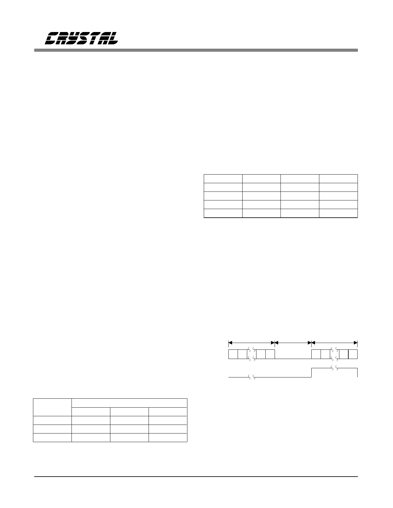
Serial Data
The serial data block consists of 20 bits of audio
data presented in 2’s-complement format with
the MSB-first, followed by 4 bits of zero and 8
Peak Signal Level, PSL, bits as shown in Fig-
ure 2. The data is clocked from SDATA by the
serial clock and the channel is determined by the
Left/Right clock.
20 Audio
Data Bits
4 Zeros
8 PSL Bits
SDATA 19 18 1 0
P7 P6 P1 P0
FRAME
Figure 2. Data Block and Frame
DS237PP2
7
Share Link: 