CS4927-CL Просмотр технического описания (PDF) - Cirrus Logic
Номер в каталоге
Компоненты Описание
Список матч
CS4927-CL Datasheet PDF : 56 Pages
| |||
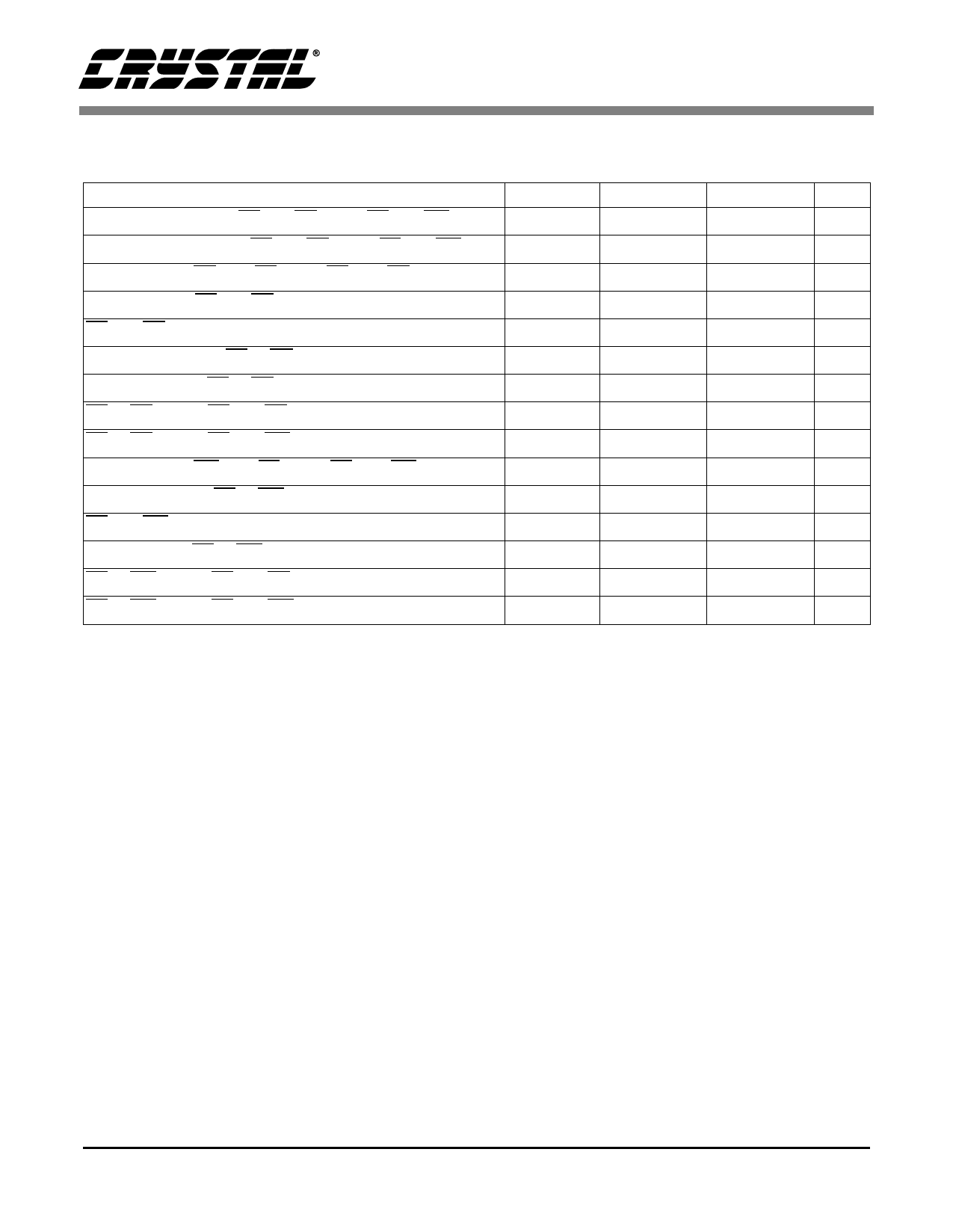
CS4923/4/5/6/7/8/9
SWITCHING CHARACTERISTICS—INTEL® HOST MODE
(TA = 25 °C; VA, VD = 3.3 V ±5%; Inputs: Logic 0 = DGND, Logic 1 = VD, CL = 20 pF)
Parameter
Symbol
Min
Max
Unit
Address setup before CS and RD low or CS and WR low
Tias
5
-
ns
Address hold time after CS and RD low or CS and WR low
Tiah
5
Delay between RD then CS low or CS then RD low
Ticdr
0
-
ns
∞
ns
Data valid after CS and RD low
Tidd
-
20
ns
CS and RD low for read
(Note 1) Tirpw
DCLK + 10
-
ns
Data hold time after CS or RD high
Tidhr
5
-
ns
Data high-Z after CS or RD high
(Note 2)
Tidis
-
15
ns
CS or RD high to CS and RD low for next read
(Note 1)
Tird
2*DCLK + 10
-
ns
CS or RD high to CS and WR low for next write (Note 1) Tirdtw
2*DCLK + 10
-
ns
Delay between WR then CS low or CS then WR low
Ticdw
0
∞
ns
Data setup before CS or WR high
Tidsu
20
-
ns
CS and WR low for write
(Note 1) Tiwpw
DCLK + 10
-
ns
Data hold after CS or WR high
Tidhw
5
-
ns
CS or WR high to CS and RD low for next read
(Note 1) Tiwtrd
2*DCLK + 10
-
ns
CS or WR high to CS and WR low for next write (Note 1) Tiwd
2*DCLK + 10
-
ns
Notes: 1. Certain timing parameters are normalized to the DSP clock, DCLK, in nanoseconds. The DSP clock can
be defined as follows:
External CLKIN Mode:
DCLK == CLKIN/3 before and during boot
DCLK == CLKIN after boot
Internal Clock Mode:
DCLK == 10MHz before and during boot, i.e. DCLK == 100ns
DCLK == 60 MHz after boot, i.e. DCLK == 16.7ns (this speed may depend on CLKIN, please see
CS4923/4/5/6/7/8/9 Hardware User’s Guide for more information)
2. This specification is characterized but not production tested.
8
DS262F2
Share Link: 