MSM7510GS-K Просмотр технического описания (PDF) - Oki Electric Industry
Номер в каталоге
Компоненты Описание
Список матч
MSM7510GS-K Datasheet PDF : 12 Pages
| |||
Semiconductor
MSM7510
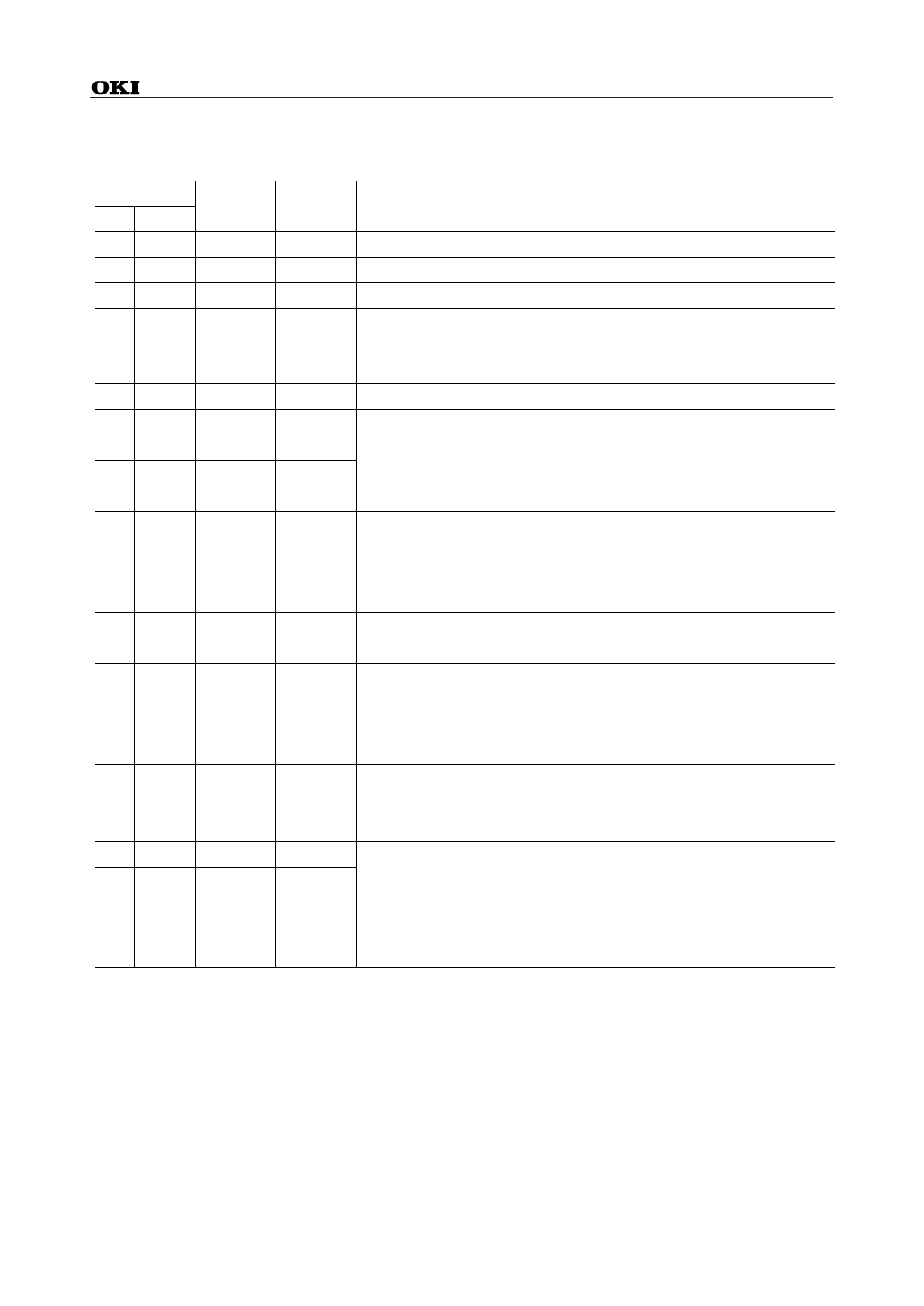
PIN DESCRIPTION
No.
Name
I/O
RS GS-VK
Description
1
1
VDD
2
3
AI
—
+3 V to +5 V Power Supply
I
Analog receive signal input.
3
5
AO
O
Analog transmit signal output.
External analog signal input.
4
6
EAI
I
The signal applied to this pin is transmitted from AO via transmit output
amplifier. When not using this pin, it should be left opened.
5
7
GND
—
Ground, 0 V.
6
8
X1
3.579545 MHz crystal resonator should be connected to X1 and X2.
I
When applying external clock 3.579545 MHz to the device, it should be
7 10
X2
applied to X2 (not X1) via an AC-coupling capacitor of 100 pF and X1
O
has to be opened.
8 12
CLK
O
3.579545 MHz clock signal output.
Modem receive serial data output.
9 13
RD
O
Digital "1" and "0" correspond to "Mark" and "Space", respectively. When
CD (Carrier Detect) is off, RD is held at "Mark" state.
10 15
CD
FSK receive signal and answer tone detect.
O
Digital "0" and "1" represent "Detect" and "Non-detect", respectively.
11 17
XD
Modem transmit serial data input.
I*
Digital "1" and "0" correspond to "Mark" and "Space", respectively.
12 18
RS
FSK signal and answer tone transmit enable.
I*
When digital "0" is applied to RS, transmitting becomes enable.
Originate/Answer mode select.
13 19
O/A
I*
Digital "1" Æ Originate mode
Digital "0" Æ Answer mode
14 20
MOD1
I*
Operation mode select.
15 22
MOD2
I*
Refer to Table 1.
Analog transmit signal amplitude select.
16 24
AOG
I*
Digital "1" Æ –10 dBm Typ. at AO
Digital "0" Æ –4 dBm Typ. at AO
Note : I* : Internally pulled-up input pin.
4/12
Share Link: 