CDP1872 Просмотр технического описания (PDF) - Intersil
Номер в каталоге
Компоненты Описание
Список матч
CDP1872 Datasheet PDF : 6 Pages
| |||
CDP1872C, CDP1874C, CDP1875C
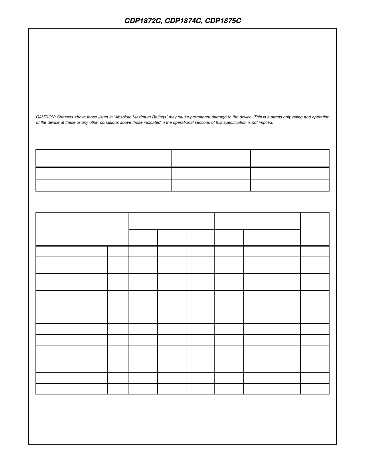
Absolute Maximum Ratings
Thermal Information
DC Supply Voltage Range, (VDD) . . . . . . . . . . . . . . . . . -0.5V to +7V
(Voltage referenced to VSS Terminal)
Input Voltage Range, All Inputs . . . . . . . . . . . . . -0.5V to VDD +0.5V
DC Input Current, Any One Input. . . . . . . . . . . . . . . . . . . . . . . . .±10mA
Thermal Resistance (Typical)
θJA (oC/W)
PDIP Package . . . . . . . . . . . . . . . . . . . . . . . . . . . . .
75
Device Dissipation Per Output Transistor
TA = Full Package Temperature Range
(All Package Types) . . . . . . . . . . . . . . . . . . . . . . . . . . . . . . 100mW
Operating Temperature Range (TA)
Package Type E . . . . . . . . . . . . . . . . . . . . . . . . . . . -40oC to +85oC
Storage Temperature Range (TSTG) . . . . . . . . . . . . -65oC to +150oC
Lead Temperature (During Soldering)
At distance 1/16 ± 1/32 In. (1.59 ± 0.79mm)
from case for 10s max . . . . . . . . . . . . . . . . . . . . . . . . . . . . +265oC
CAUTION: Stresses above those listed in “Absolute Maximum Ratings” may cause permanent damage to the device. This is a stress only rating and operation
of the device at these or any other conditions above those indicated in the operational sections of this specification is not implied.
Recommended Operating Conditions At TA = -40 to +85oC. For maximum reliability, operating conditions should be selected
so that operation is always within the following ranges:
PARAMETER
LIMITS
ALL TYPES
UNITS
DC Operating-Voltage Range
4 to 6.5
V
Input Voltage Range
VSS to VDD
V
Static Electrical Specifications At TA = -40 to +85oC, VDD ±5%, Unless Otherwise Specified.
TEST CONDITIONS
LIMITS
ALL TYPES
PARAMETER
VO
VIN
VDD
(NOTE 1)
(V)
(V)
(V)
MIN
TYP
Quiescent Device Current
IDD
-
0, 5
5
Output Low Drive (Sink)
Current
IOL
0.4
0, 5
5
-
25
5
10
Output High Drive (Source)
IOH
4.6
0, 5
5
Current
-4
-7
Output Voltage Low-Level
VOL
-
0, 5
5
-
0
(Note 2)
Output Voltage High-Level
VOH
-
0, 5
5
4.9
5
(Note 2)
Input Low Voltage
VIL
0.5, 4.5
-
5
-
-
Input High Voltage
VIH
0.5, 4.5
-
5
3.5
-
Input Leakage Current
IIN
-
0, 5
5
-
-
Three-State Output Leakage
IOUT
0, 5
0, 5
5
-
-
Current (Note 3)
Input Capacitance
CIN
-
-
-
-
15
Output Capacitance (Note 3)
COUT
-
-
-
-
15
NOTES:
1. Typical values are for TA = +25oC and nominal VDD ±5%.
2. IOL = IOH = 1µA
3. For CDP1872C and CDP1874C only.
MAX
50
-
-
0.1
-
1.5
-
±1
±5
-
-
UNITS
µA
mA
mA
V
V
V
V
µA
µA
pF
pF
4-77
Share Link: 